SNVSAR1B March 2017 – March 2018 LM5113-Q1
PRODUCTION DATA.
- 1 Features
- 2 Applications
- 3 Description
- 4 Revision History
- 5 Pin Configuration and Functions
- 6 Specifications
- 7 Detailed Description
- 8 Application and Implementation
- 9 Power Supply Recommendations
- 10Layout
- 11Device and Documentation Support
- 12Mechanical, Packaging, and Orderable Information
Package Options
Mechanical Data (Package|Pins)
- DPR|10
Thermal pad, mechanical data (Package|Pins)
Orderable Information
6.7 Typical Characteristics
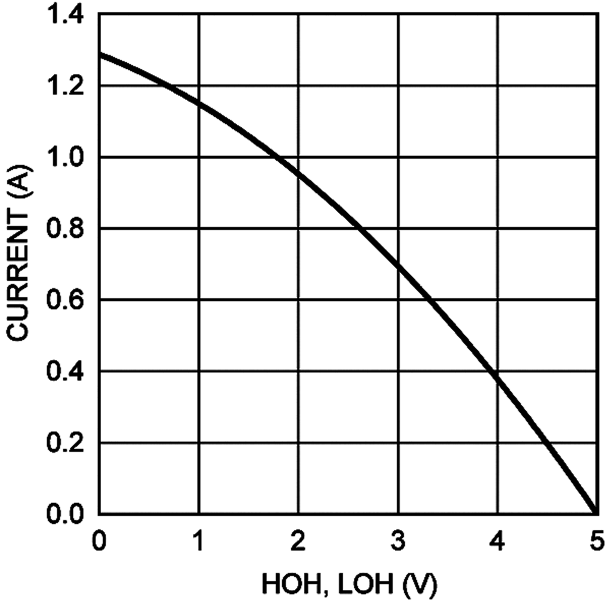 Figure 2. Peak Source Current vs Output Voltage
 Figure 4. IDDO vs Frequency
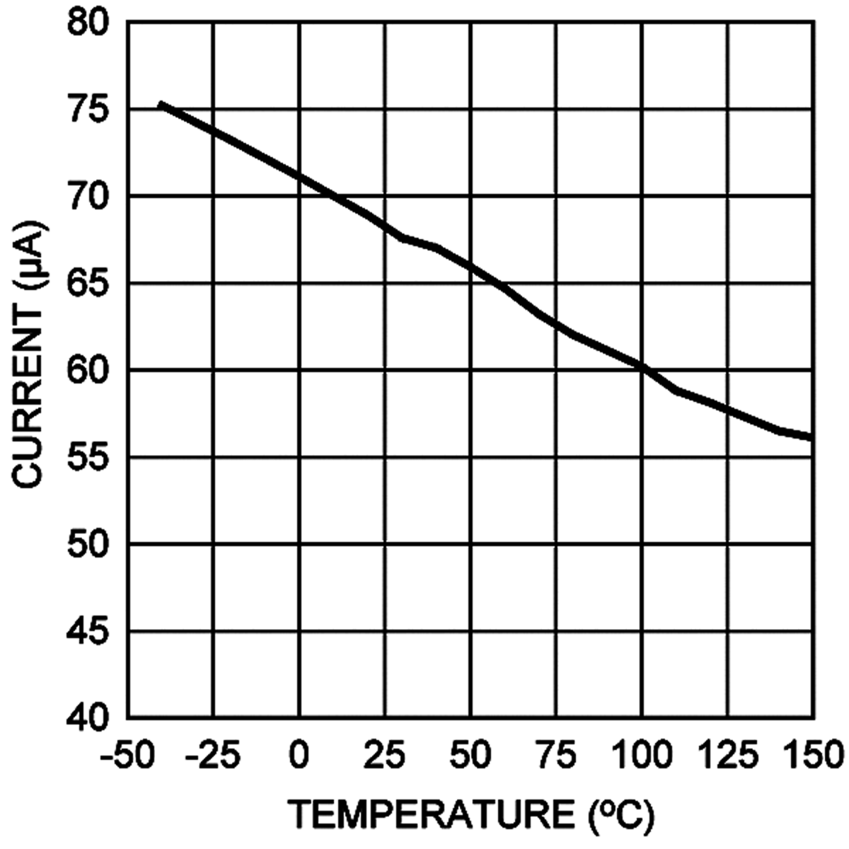 Figure 6. IDD vs Temperature
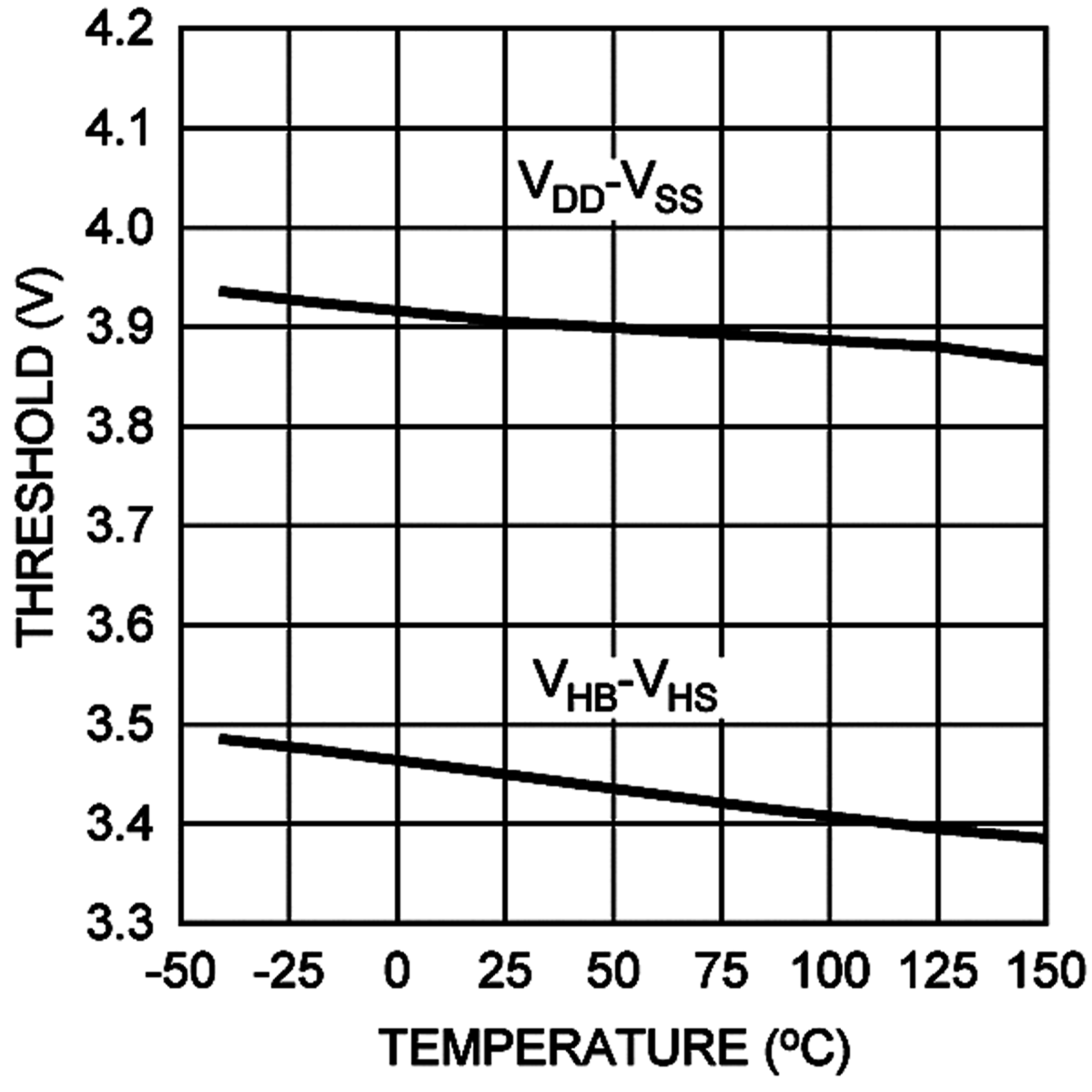 Figure 8. UVLO Rising Thresholds vs Temperature
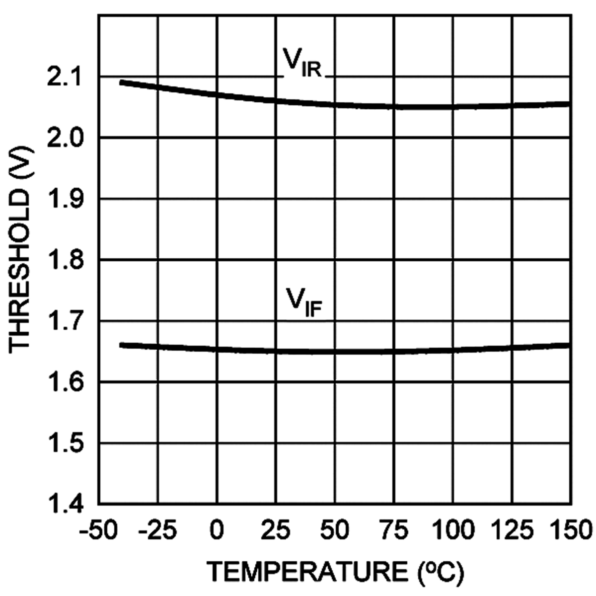 Figure 10. Input Thresholds vs Temperature
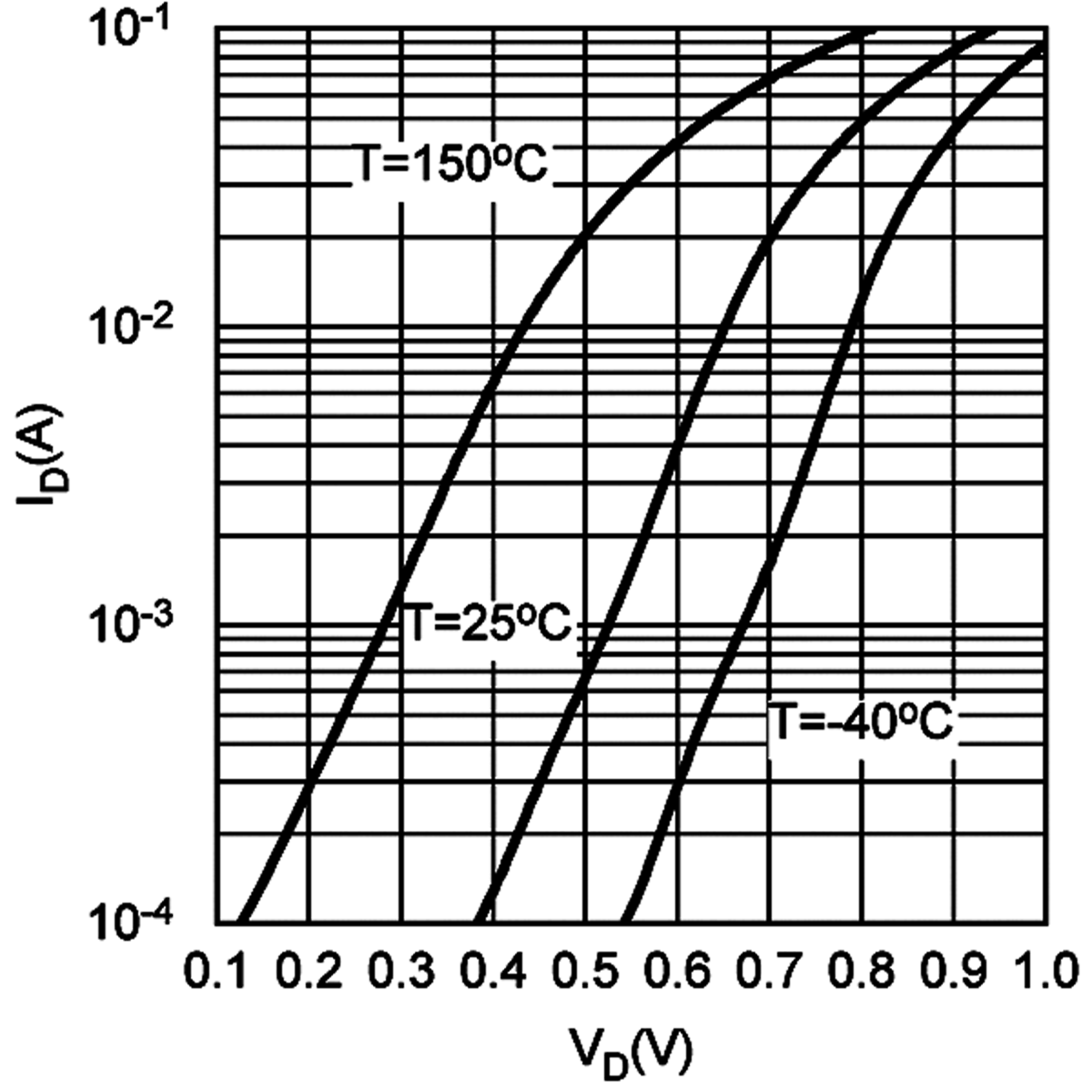 Figure 12. Bootstrap Diode Forward Voltage
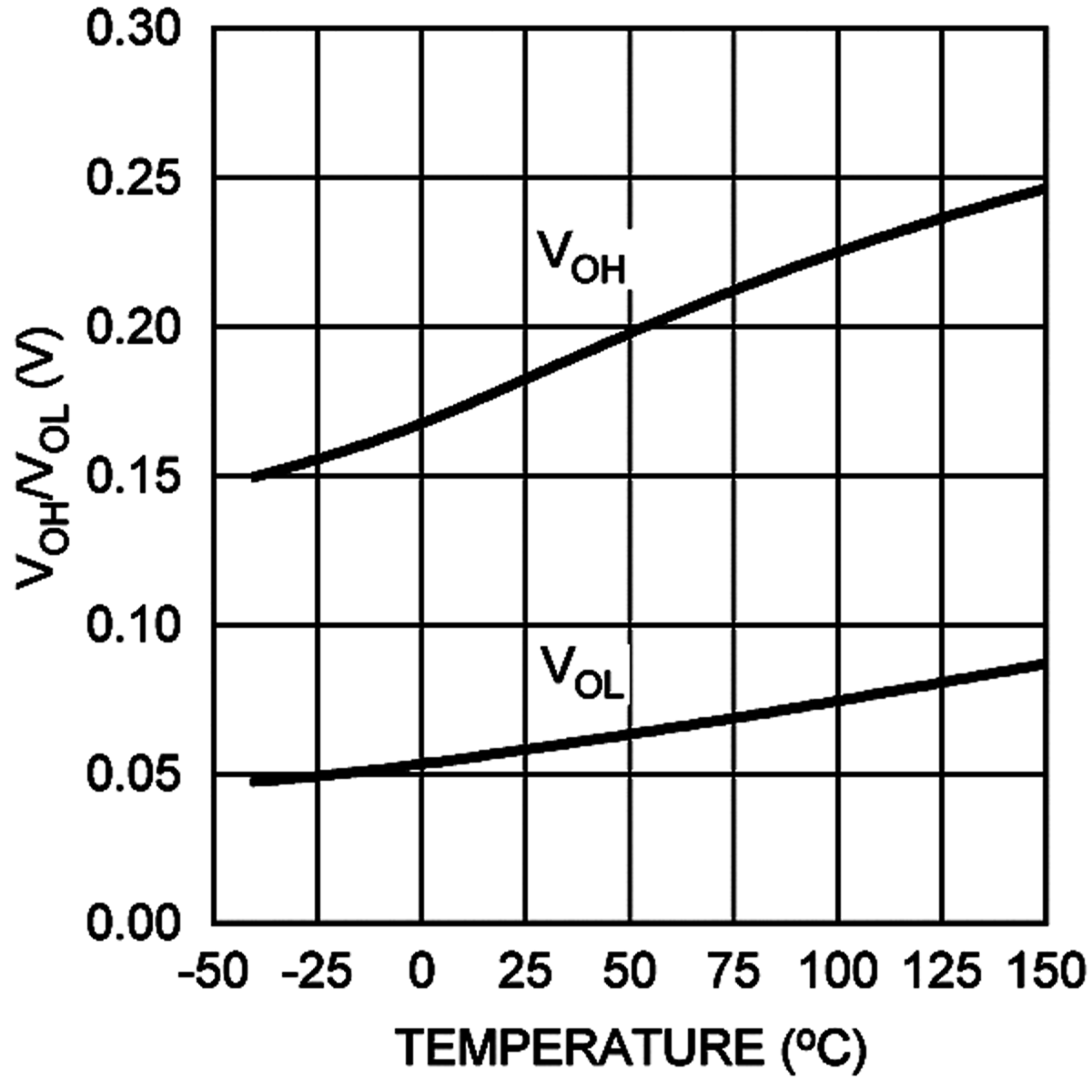
| Note: Unless otherwise specified, VDD = VHB = 5 V,
VSS = VHS = 0 V. |
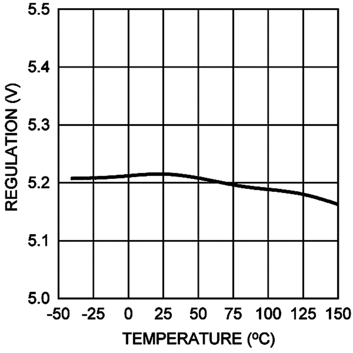
Output Voltage vs Temperature
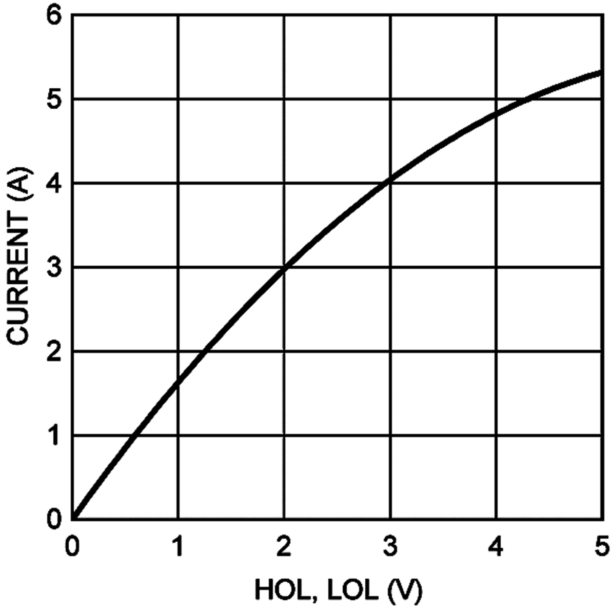 Figure 3. Peak Sink Current vs Output Voltage
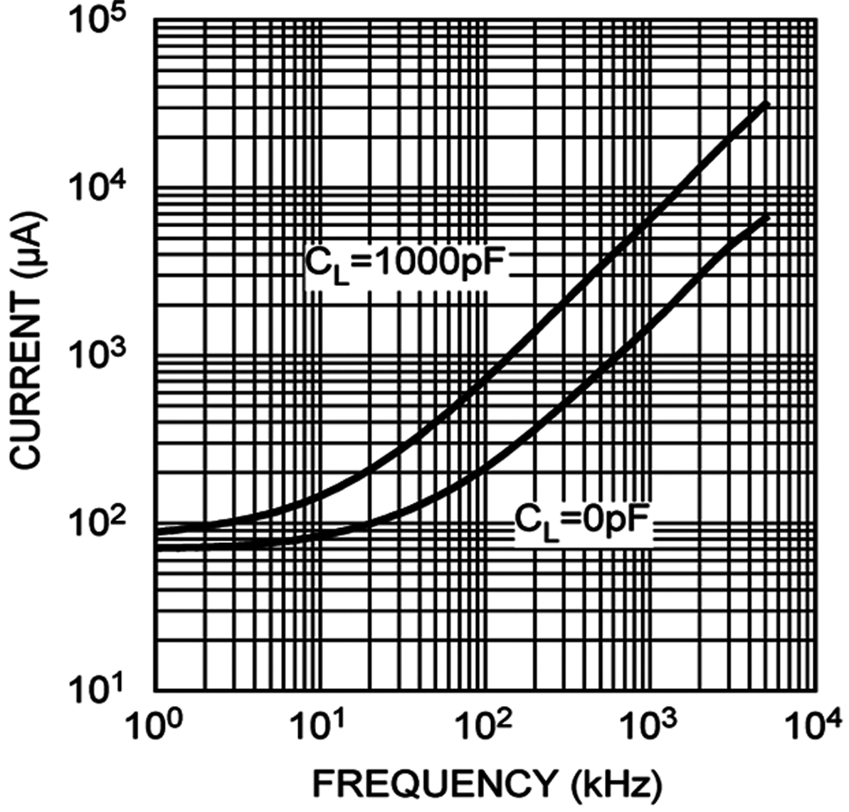 Figure 5. IHBO vs Frequency
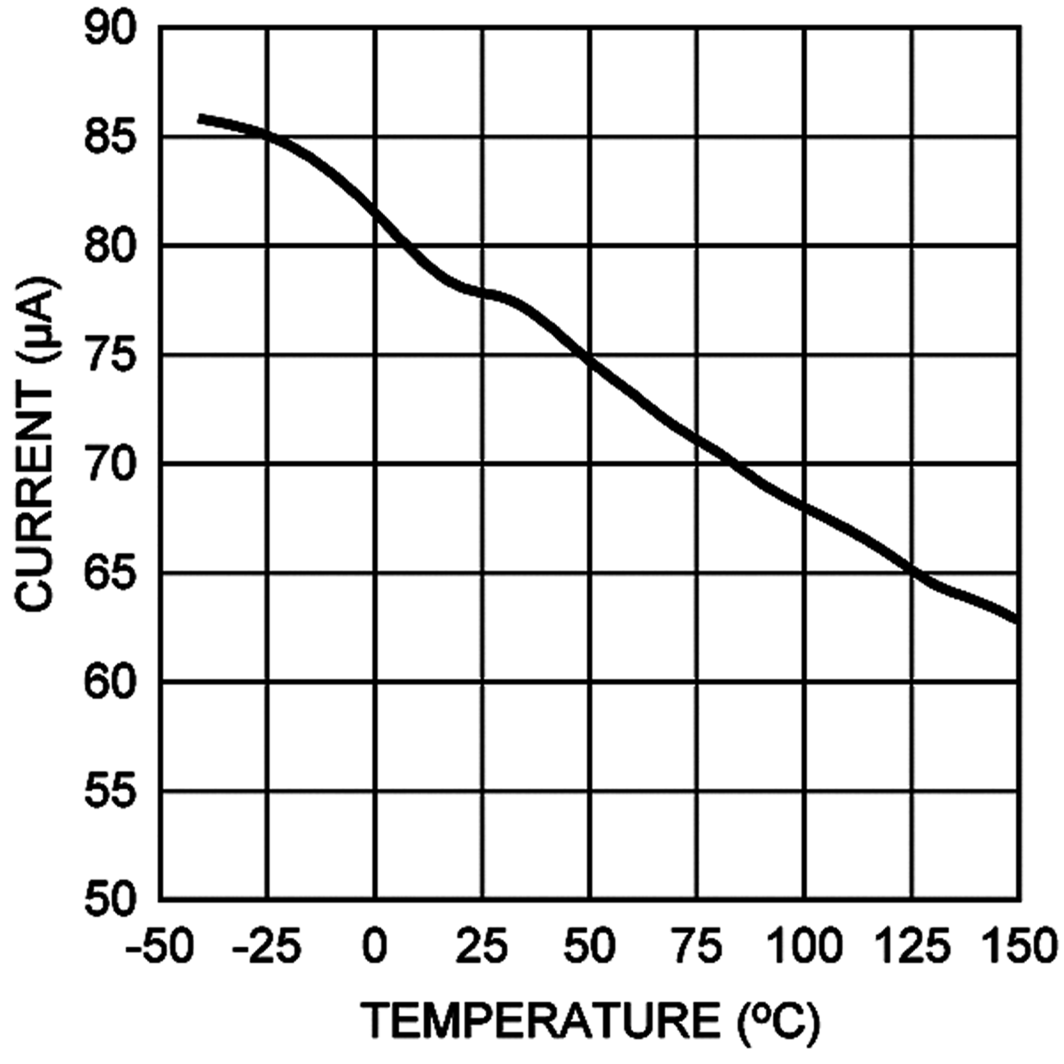 Figure 7. IHB vs Temperature
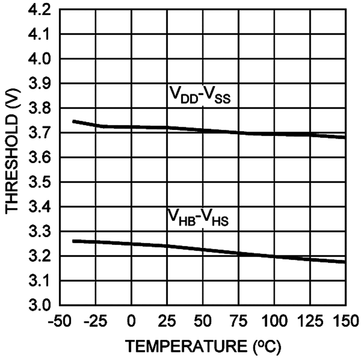 Figure 9. UVLO Falling Thresholds vs Temperature
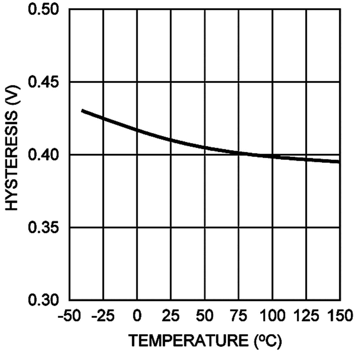 Figure 11. Input Threshold Hysteresis vs Temperature
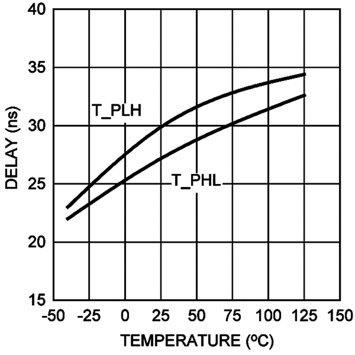 Figure 13. Propagation Delay vs Temperature
