SNVS499I February 2007 – November 2023 LM5116
PRODUCTION DATA
- 1
- 1 Features
- 2 Applications
- 3 Description
- 4 Pin Configuration and Functions
- 5 Specifications
- 6 Detailed Description
-
7 Application and Implementation
- 7.1 Application Information
- 7.2
Typical Application
- 7.2.1 Design Requirements
- 7.2.2
Detailed Design Procedure
- 7.2.2.1 Custom Design with WEBENCH® Tools
- 7.2.2.2 Timing Resistor
- 7.2.2.3 Output Inductor
- 7.2.2.4 Current Sense Resistor
- 7.2.2.5 Ramp Capacitor
- 7.2.2.6 Output Capacitors
- 7.2.2.7 Input Capacitors
- 7.2.2.8 VCC Capacitor
- 7.2.2.9 Bootstrap Capacitor
- 7.2.2.10 Soft Start Capacitor
- 7.2.2.11 Output Voltage Divider
- 7.2.2.12 UVLO Divider
- 7.2.2.13 MOSFETs
- 7.2.2.14 MOSFET Snubber
- 7.2.2.15 Error Amplifier Compensation
- 7.2.2.16 Comprehensive Equations
- 7.2.3 Application Curves
- 7.3 Power Supply Recommendations
- 7.4 Layout
- 8 Device and Documentation Support
- 9 Revision History
- 10Mechanical, Packaging, and Orderable Information
Package Options
Mechanical Data (Package|Pins)
- PWP|20
Thermal pad, mechanical data (Package|Pins)
- PWP|20
Orderable Information
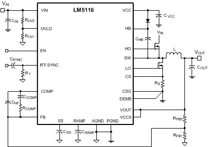
3 Description
The LM5116 is a synchronous buck controller intended for step-down regulator applications from a high-voltage or widely varying input supply. The control method is based upon current mode control using an emulated current ramp. Current mode control provides inherent line feed-forward, cycle-by-cycle current limiting, and ease-of-loop compensation. The use of an emulated control ramp reduces noise sensitivity of the pulse-width modulation circuit, allowing reliable control of very small duty cycles necessary in high-input voltage applications.
The operating frequency is programmable from 50 kHz to 1 MHz. The LM5116 drives external high-side and low-side NMOS power switches with adaptive dead-time control. A user-selectable diode emulation mode enables discontinuous mode operation, for improved efficiency at light load conditions. A low quiescent current shutdown disables the controller and consumes less than 10 µA of total input current.
Additional features include a high-voltage bias regulator, automatic switch-over to external bias for improved efficiency, thermal shutdown, frequency synchronization, cycle-by-cycle current limit, and adjustable line undervoltage lockout. The device is available in a power enhanced HTSSOP-20 package featuring an exposed die attach pad to aid thermal dissipation.
New products (LM5148 and LM5149) offer reduced BOM cost, higher efficiency, and reduced design size among many other features.
 Typical
Application