SNVS676I August 2010 – April 2018 LM5119
PRODUCTION DATA.
- 1 Features
- 2 Applications
- 3 Description
- 4 Revision History
- 5 Pin Configuration and Functions
- 6 Specifications
-
7 Detailed Description
- 7.1 Overview
- 7.2 Functional Block Diagram
- 7.3
Feature Description
- 7.3.1 High Voltage Start-Up Regulator
- 7.3.2 UVLO
- 7.3.3 Enable 2
- 7.3.4 Oscillator and Sync Capability
- 7.3.5 Error Amplifiers and PWM Comparators
- 7.3.6 Ramp Generator
- 7.3.7 Current Limit
- 7.3.8 Hiccup Mode Current Limiting
- 7.3.9 Soft Start
- 7.3.10 HO and LO Output Drivers
- 7.3.11 Maximum Duty Cycle
- 7.3.12 Thermal Protection
- 7.4 Device Functional Modes
-
8 Application and Implementation
- 8.1 Application Information
- 8.2
Typical Applications
- 8.2.1
Dual-output Design Example
- 8.2.1.1 Design Requirements
- 8.2.1.2
Detailed Design Procedure
- 8.2.1.2.1 Timing Resistor
- 8.2.1.2.2 Output Inductor
- 8.2.1.2.3 Current Sense Resistor
- 8.2.1.2.4 Ramp Resistor and Ramp Capacitor
- 8.2.1.2.5 Output Capacitors
- 8.2.1.2.6 Input Capacitors
- 8.2.1.2.7 VCC Capacitor
- 8.2.1.2.8 Bootstrap Capacitor
- 8.2.1.2.9 Soft-Start Capacitor
- 8.2.1.2.10 Restart Capacitor
- 8.2.1.2.11 Output Voltage Divider
- 8.2.1.2.12 UVLO Divider
- 8.2.1.2.13 MOSFET Snubber
- 8.2.1.2.14 Error Amplifier Compensation
- 8.2.1.3 Application Curves
- 8.2.2 Two-Phase Design Example
- 8.2.1
Dual-output Design Example
- 9 Power Supply Recommendations
- 10Layout
- 11Device and Documentation Support
- 12Mechanical, Packaging, and Orderable Information
Package Options
Mechanical Data (Package|Pins)
- RTV|32
Thermal pad, mechanical data (Package|Pins)
- RTV|32
Orderable Information
7.3.1 High Voltage Start-Up Regulator
The LM5119 contains two internal high voltage bias regulators, VCC1 and VCC2, that provide the bias supply for the PWM controllers and gate drive for the MOSFETs of each regulator channel. The input pin (VIN) can be connected directly to an input voltage source as high as 65 V. The outputs of the VCC regulators are set to
7.6 V. When the input voltage is below the VCC set-point level, the VCC output tracks the VIN with a small dropout voltage. If VCC1 is in an undervoltage condition, channel2 is disabled. This interdependence is necessary to prevent channel2 from running open-loop in the single output interleaved mode when the channel2 error amplifier is disabled (if either VCC is in UV, both channels are disabled).
The outputs of the VCC regulators are current limited at 25-mA (minimum) output capability. Upon power up, the regulators source current into the capacitors connected to the VCC pins. When the voltage at the VCC pins exceed 4.9 V and the UVLO pin is greater than 1.25 V, both channels are enabled and a soft-start sequence begins. Both channels remain enabled until either VCC pin falls below 4.7 V, the UVLO pin falls below 1.25 V or the die temperature exceeds the thermal limit threshold.
When operating at higher input voltages the bias power dissipation within the controller can be excessive. An output voltage derived bias supply can be applied to a VCC pins to reduce the IC power dissipation. The VCCDIS input can be used to disable the internal VCC regulators when external biasing is supplied.
If VCCDIS >1.25 V, the internal VCC regulators are disabled. The externally supplied bias must be coupled to the VCC pins through a diode, preferably a Schottky (low forward voltage). VCCDIS has a 500-kΩ internal pulldown resistance to ground for normal operation with no external bias. The internal pulldown resistance can be overridden by pulling VCCDIS above 1.25 V through a resistor divider connected to an external bias supply.
The VCC regulator series pass transistor includes a diode between VCC and VIN that must not be forward biased in normal operation.
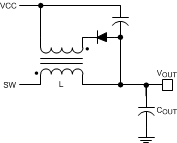
If the external bias winding can supply VCC greater than VIN, an external blocking diode is required from the input power supply to the VIN pin to prevent the external bias supply from passing current to the input supply through the VCC pins. For VOUT between 6 V and 14.5 V, VOUT can be connected directly to VCC through a diode. For VOUT < 6 V, a bias winding on the output inductor can be added as shown in Figure 8.
 Figure 8. VCC Bias Supply With Additional Inductor Winding
In high voltage applications, take extra care to ensure the VIN pin does not exceed the absolute maximum voltage rating of 75 V. During line or load transients, voltage ringing on the VIN line that exceeds the Absolute Maximum Rating can damage the IC. Both careful PCB layout and the use of quality bypass capacitors placed close to the VIN and AGND pins are essential.