SNVS954H February 2013 – June 2017 LM5122
PRODUCTION DATA.
- 1 Features
- 2 Applications
- 3 Description
- 4 Revision History
- 5 Pin Configuration and Functions
- 6 Specifications
-
7 Detailed Description
- 7.1 Overview
- 7.2 Functional Block Diagram
- 7.3
Feature Description
- 7.3.1 Undervoltage Lockout (UVLO)
- 7.3.2 High Voltage VCC Regulator
- 7.3.3 Oscillator
- 7.3.4 Slope Compensation
- 7.3.5 Error Amplifier
- 7.3.6 PWM Comparator
- 7.3.7 Soft-Start
- 7.3.8 HO and LO Drivers
- 7.3.9 Bypass Operation (VOUT = VIN)
- 7.3.10 Cycle-by-Cycle Current Limit
- 7.3.11 Clock Synchronization
- 7.3.12 Maximum Duty Cycle
- 7.3.13 Thermal Protection
- 7.4 Device Functional Modes
-
8 Application and Implementation
- 8.1
Application Information
- 8.1.1 Feedback Compensation
- 8.1.2 Sub-Harmonic Oscillation
- 8.1.3 Interleaved Boost Configuration
- 8.1.4 DCR Sensing
- 8.1.5 Output Overvoltage Protection
- 8.1.6 SEPIC Converter Simplified Schematic
- 8.1.7 Non-Isolated Synchronous Flyback Converter Simplified Schematic
- 8.1.8 Negative to Positive Conversion
- 8.2
Typical Application
- 8.2.1 Design Requirements
- 8.2.2
Detailed Design Procedure
- 8.2.2.1 Custom Design With WEBENCH® Tools
- 8.2.2.2 Timing Resistor RT
- 8.2.2.3 UVLO Divider RUV2, RUV1
- 8.2.2.4 Input Inductor LIN
- 8.2.2.5 Current Sense Resistor RS
- 8.2.2.6 Current Sense Filter RCSFP, RCSFN, CCS
- 8.2.2.7 Slope Compensation Resistor RSLOPE
- 8.2.2.8 Output Capacitor COUT
- 8.2.2.9 Input Capacitor CIN
- 8.2.2.10 VIN Filter RVIN, CVIN
- 8.2.2.11 Bootstrap Capacitor CBST and Boost Diode DBST
- 8.2.2.12 VCC Capacitor CVCC
- 8.2.2.13 Output Voltage Divider RFB1, RFB2
- 8.2.2.14 Soft-Start Capacitor CSS
- 8.2.2.15 Restart Capacitor CRES
- 8.2.2.16 Low-Side Power Switch QL
- 8.2.2.17 High-Side Power Switch QH and Additional Parallel Schottky Diode
- 8.2.2.18 Snubber Components
- 8.2.2.19 Loop Compensation Components CCOMP, RCOMP, CHF
- 8.2.3 Application Curves
- 8.1
Application Information
- 9 Power Supply Recommendations
- 10Layout
- 11Device and Documentation Support
- 12Mechanical, Packaging, and Orderable Information
Package Options
Mechanical Data (Package|Pins)
Thermal pad, mechanical data (Package|Pins)
Orderable Information
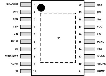
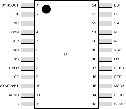
5 Pin Configuration and Functions
PWP Package
20-Pin HTSSOP With Exposed Pad
Top View

Pin Functions
| PIN | TYPE(1) | DESCRIPTION | ||
|---|---|---|---|---|
| NAME | 24-Pin | 20-Pin | ||
| AGND | 11 | 9 | G | Analog ground connection. Return for the internal voltage reference and analog circuits. |
| BST | 24 | 20 | P | High-side driver supply for bootstrap gate drive. Connect to the cathode of the external bootstrap diode and to the bootstrap capacitor. The bootstrap capacitor supplies current to charge the high-side N-channel MOSFET gate and should be placed as close to controller as possible. An internal BST charge pump supplies 200-µA current into bootstrap capacitor for bypass operation. |
| COMP | 13 | 11 | O | Output of the internal error amplifier. Connect the loop compensation network between this pin and the FB pin. |
| CSN | 4 | 3 | I | Inverting input of current sense amplifier. Connect to the negative-side of the current sense resistor. |
| CSP | 5 | 4 | I | Non-inverting input of current sense amplifier. Connect to the positive-side of the current sense resistor. |
| FB | 12 | 10 | I | Feedback. Inverting input of the internal error amplifier. A resistor divider from the output to this pin sets the output voltage level. The regulation threshold at the FB pin is 1.2 V. The controller is configured as slave mode if the FB pin voltage is above 2.7 V at initial power-on. |
| HO | 23 | 19 | O | High-side N-channel MOSFET gate drive output. Connect to the gate of the high-side synchronous N-channel MOSFET switch through a short, low inductance path. |
| LO | 18 | 16 | O | Low-side N-channel MOSFET gate drive output. Connect to the gate of the low-side N-channel MOSFET switch through a short, low inductance path. |
| MODE | 15 | 13 | I | Switching mode selection pin. 700-kΩ pullup and 100-kΩ pulldown resistor internal hold MODE pin to 0.15 V as a default. By adding external pullup or pulldown resistor, MODE pin voltage can be programmed. When MODE pin voltage is greater than 1.2-V diode emulation mode threshold, forced PWM mode is enabled, allowing current to flow in either direction through the high-side N-channel MOSFET switch. When MODE pin voltage is less than 1.2 V, the controller works in diode emulation mode. Skip cycle comparator is activated as a default. If MODE pin is grounded, the controller still operates in diode emulation mode, but the skip cycle comparator will not be triggered in normal operation, this enables pulse skipping operation at light load. |
| OPT | 2 | 2 | I | Clock synchronization selection pin. This pin also enables/disables SYNCOUT related with master/slave configuration. The OPT pin should not be left floating. |
| PGND | 17 | 15 | G | Power ground connection pin for low-side N-channel MOSFET gate driver. Connect directly to the source terminal of the low-side N-channel MOSFET switch. |
| RES | 16 | 14 | O | The restart timer pin for an external capacitor that configures hiccup mode off-time and restart delay during over load conditions. Connect directly to the AGND when hiccup mode operation is not required. |
| SLOPE | 14 | 12 | I | Slope compensation is programmed by a single resistor between SLOPE and the AGND. |
| SS | 9 | 7 | I | Soft-start programming pin. An external capacitor and an internal 10-μA current source set the ramp rate of the internal error amplifier reference during soft-start. |
| SW | 22 | 18 | I/O | Switching node of the boost regulator. Connect to the bootstrap capacitor, the source terminal of the high-side N-channel MOSFET switch and the drain terminal of the low-side N-channel MOSFET switch through short, low inductance paths. |
| SYNCIN/RT | 10 | 8 | I | The internal oscillator frequency is programmed by a single resistor between RT and the AGND. The internal oscillator can be synchronized to an external clock by applying a positive pulse signal into this SYNCIN pin. The recommended maximum internal oscillator frequency in master configuration is 2 MHz which leads to 1 MHz maximum switching frequency. |
| SYNCOUT | 1 | 1 | O | Clock output pin. SYNCOUT provides 180° shifted clock output for an interleaved operation. SYNCOUT pin can be left floating when it is not used. See Slave Mode and SYNCOUT section. |
| UVLO | 8 | 6 | I | Undervoltage lockout programming pin. If the UVLO pin is below 0.4 V, the regulator is in the shutdown mode with all functions disabled. If the UVLO pin voltage is greater than 0.4 V and below 1.2 V, the regulator is in standby mode with the VCC regulator operational and no switching at the HO and LO outputs. If the UVLO pin voltage is above 1.2 V, the start-up sequence begins. A 10-μA current source at UVLO pin is enabled when UVLO exceeds 1.2 V and flows through the external UVLO resistors to provide hysteresis. The UVLO pin should not be left floating. |
| VCC | 19 | 17 | P/O/I | VCC bias supply pin. Locally decouple to PGND using a low ESR/ESL capacitor located as close as possible to controller. |
| VIN | 6 | 5 | P/I | Supply voltage input source for the VCC regulator. Connect to input capacitor and source power supply connection with short, low impedance paths. |
| EP | EP | N/A | Exposed pad of the package. No internal electrical connections. Must be soldered to the large ground plane to reduce thermal resistance. | |
| NC | 3, 7, 20, 21 | — | No electrical contact | |
(1) G = Ground, I = Input, O = Output, P = Power
