SNVS954H February   2013  – June 2017 LM5122

PRODUCTION DATA.  

  1. Features
  2. Applications
  3. Description
  4. Revision History
  5. Pin Configuration and Functions
  6. Specifications
    1. 6.1 Absolute Maximum Ratings
    2. 6.2 ESD Ratings: LM5122, LM5122Z
    3. 6.3 Recommended Operating Conditions
    4. 6.4 Thermal Information
    5. 6.5 Electrical Characteristics
    6. 6.6 Typical Characteristics
  7. Detailed Description
    1. 7.1 Overview
    2. 7.2 Functional Block Diagram
    3. 7.3 Feature Description
      1. 7.3.1  Undervoltage Lockout (UVLO)
      2. 7.3.2  High Voltage VCC Regulator
      3. 7.3.3  Oscillator
      4. 7.3.4  Slope Compensation
      5. 7.3.5  Error Amplifier
      6. 7.3.6  PWM Comparator
      7. 7.3.7  Soft-Start
      8. 7.3.8  HO and LO Drivers
      9. 7.3.9  Bypass Operation (VOUT = VIN)
      10. 7.3.10 Cycle-by-Cycle Current Limit
      11. 7.3.11 Clock Synchronization
      12. 7.3.12 Maximum Duty Cycle
      13. 7.3.13 Thermal Protection
    4. 7.4 Device Functional Modes
      1. 7.4.1 MODE Control (Forced-PWM Mode and Diode-Emulation Mode)
      2. 7.4.2 MODE Control (Skip-Cycle Mode and Pulse-Skipping Mode)
      3. 7.4.3 Hiccup-Mode Overload Protection
      4. 7.4.4 Slave Mode and SYNCOUT
  8. Application and Implementation
    1. 8.1 Application Information
      1. 8.1.1 Feedback Compensation
      2. 8.1.2 Sub-Harmonic Oscillation
      3. 8.1.3 Interleaved Boost Configuration
      4. 8.1.4 DCR Sensing
      5. 8.1.5 Output Overvoltage Protection
      6. 8.1.6 SEPIC Converter Simplified Schematic
      7. 8.1.7 Non-Isolated Synchronous Flyback Converter Simplified Schematic
      8. 8.1.8 Negative to Positive Conversion
    2. 8.2 Typical Application
      1. 8.2.1 Design Requirements
      2. 8.2.2 Detailed Design Procedure
        1. 8.2.2.1  Custom Design With WEBENCH® Tools
        2. 8.2.2.2  Timing Resistor RT
        3. 8.2.2.3  UVLO Divider RUV2, RUV1
        4. 8.2.2.4  Input Inductor LIN
        5. 8.2.2.5  Current Sense Resistor RS
        6. 8.2.2.6  Current Sense Filter RCSFP, RCSFN, CCS
        7. 8.2.2.7  Slope Compensation Resistor RSLOPE
        8. 8.2.2.8  Output Capacitor COUT
        9. 8.2.2.9  Input Capacitor CIN
        10. 8.2.2.10 VIN Filter RVIN, CVIN
        11. 8.2.2.11 Bootstrap Capacitor CBST and Boost Diode DBST
        12. 8.2.2.12 VCC Capacitor CVCC
        13. 8.2.2.13 Output Voltage Divider RFB1, RFB2
        14. 8.2.2.14 Soft-Start Capacitor CSS
        15. 8.2.2.15 Restart Capacitor CRES
        16. 8.2.2.16 Low-Side Power Switch QL
        17. 8.2.2.17 High-Side Power Switch QH and Additional Parallel Schottky Diode
        18. 8.2.2.18 Snubber Components
        19. 8.2.2.19 Loop Compensation Components CCOMP, RCOMP, CHF
      3. 8.2.3 Application Curves
  9. Power Supply Recommendations
  10. 10Layout
    1. 10.1 Layout Guidelines
    2. 10.2 Layout Example
  11. 11Device and Documentation Support
    1. 11.1 Device Support
      1. 11.1.1 Development Support
        1. 11.1.1.1 Custom Design With WEBENCH® Tools
    2. 11.2 Receiving Notification of Documentation Updates
    3. 11.3 Community Resources
    4. 11.4 Trademarks
    5. 11.5 Electrostatic Discharge Caution
    6. 11.6 Glossary
  12. 12Mechanical, Packaging, and Orderable Information

Package Options

Mechanical Data (Package|Pins)
Thermal pad, mechanical data (Package|Pins)
Orderable Information

Specifications

Absolute Maximum Ratings

Over operating free-air temperature range (unless otherwise noted)(1)
MIN MAX UNIT
Input VIN, CSP, CSN –0.3 75 V
BST to SW, FB, MODE, UVLO, OPT, VCC(2) –0.3 15 V
SW –5 105 V
BST –0.3 115 V
SS, SLOPE, SYNCIN/RT –0.3 7 V
CSP to CSN, PGND –0.3 0.3 V
Output(3) HO to SW –0.3 BST to SW + 0.3 V
LO –0.3 VCC + 0.3 V
COMP, RES, SYNCOUT –0.3 7 V
Thermal Junction temperature –40 150 °C
Storage temperature, Tstg –55 150 °C
Stresses beyond those listed under Absolute Maximum Ratings may cause permanent damage to the device. These are stress ratings only and functional operation of the device at these or any other conditions beyond those indicated under Recommended Operating Conditions are not implied. Exposure to absolute-maximum-rated conditions for extended periods may affect device reliability. Unless otherwise specified, all voltages are referenced to AGND pin.
See Application and Implementation when input supply voltage is less than the VCC voltage.
All output pins are not specified to have an external voltage applied.

ESD Ratings: LM5122, LM5122Z

VALUE UNIT
V(ESD) Electrostatic discharge Human body model (HBM), per JESD22-A114 (1) ±2000 V
Charged device model (CDM), per JESD22-C101 (2) ±1000
JEDEC document JEP155 states that 500-V HBM allows safe manufacturing with a standard ESD control process.
JEDEC document JEP157 states that 250-V CDM allows safe manufacturing with a standard ESD control process.

Recommended Operating Conditions

over operating free-air temperature range (unless otherwise noted)(1)
MIN MAX UNIT
Input supply voltage(2) VIN 4.5 65 V
Low-side driver bias voltage VCC 14 V
High-side driver bias voltage BST to SW 3.8 14 V
Current sense common mode range(2) CSP, CSN 3 65 V
Switch node voltage SW 100 V
Junction temperature, TJ –40 125 °C
Recommended Operating Conditions are conditions under which operation of the device is intended to be functional, but do not ensure specific performance limits.
Minimum VIN operating voltage is always 4.5 V. The minimum input power supply voltage can be 3 V after start-up, assuming VIN voltage is supplied from an available external source.

Thermal Information

THERMAL METRIC LM5122, LM5122Z UNIT
PWP
20 PINS 24 PINS
RθJA Junction-to-ambient thermal resistance 36 32.4 °C/W
RθJC(top) Junction-to-case (top) thermal resistance 20.1 15.6 °C/W
RθJB Junction-to-board thermal resistance 16.8 7.5 °C/W
ψJT Junction-to-top characterization parameter 0.4 0.2 °C/W
ψJB Junction-to-board characterization parameter 16.7 7.7 °C/W
RθJC(bot) Junction-to-case (bottom) thermal resistance 1.7 1.1 °C/W

Electrical Characteristics

Unless otherwise specified, these specifications apply for –40°C ≤ TJ ≤ +125°C, VVIN = 12 V, VVCC = 8.3 V, RT = 20 kΩ, no load on LO and HO. Typical values represent the most likely parametric norm at TJ = 25°C and are provided for reference purposes only.
PARAMETER TEST CONDITIONS MIN TYP MAX UNIT
VIN SUPPLY
ISHUTDOWN VIN shutdown current VUVLO = 0 V 9 17 µA
IBIAS VIN operating current (exclude the current into RT resistor) VUVLO = 2 V, non-switching 4 5 mA
VCC REGULATOR
VCC(REG) VCC regulation No load 6.9 7.6 8.3 V
VCC dropout (VIN to VCC) VVIN = 4.5 V, no external load 0.25 V
VVIN = 4.5 V, IVCC = 25 mA 0.28 0.5 V
VCC sourcing current limit VVCC = 0 V 50 62 mA
IVCC VCC operating current (exclude the current into RT resistor) VVCC = 8.3 V 3.5 5 mA
VVCC = 12 V 4.5 8 mA
VCC undervoltage threshold VCC rising, VVIN = 4.5 V 3.9 4 4.1 V
VCC falling, VVIN = 4.5 V 3.7 V
VCC undervoltage hysteresis 0.385 V
UNDERVOLTAGE LOCKOUT
UVLO threshold UVLO rising 1.17 1.2 1.23 V
UVLO hysteresis current VUVLO = 1.4 V 7 10 13 µA
UVLO standby enable threshold UVLO rising 0.3 0.4 0.5 V
UVLO standby enable hysteresis 0.1 0.125 V
MODE
Diode emulation mode threshold MODE rising 1.2 1.24 1.28 V
Diode emulation mode hysteresis 0.1 V
Default MODE voltage 145 155 170 mV
Default skip cycle threshold COMP rising, measured at COMP 1.290 V
COMP falling, measured at COMP 1.245 V
Skip cycle hysteresis Measured at COMP 40 mV
ERROR AMPLIFIER
VREF FB reference voltage Measured at FB, VFB = VCOMP 1.188 1.2 1.212 V
FB input bias current VFB = VREF 5 nA
VOH COMP output high voltage ISOURCE = 2 mA, VVCC = 4.5 V 2.75 V
ISOURCE = 2 mA, VVCC = 12 V 3.4 V
VOL COMP output low voltage ISINK = 2 mA 0.25 V
AOL DC gain 80 dB
fBW Unity gain bandwidth 3 MHz
Slave mode threshold FB rising 2.7 3.4 V
OSCILLATOR
fSW1 Switching frequency 1 RT = 20 kΩ 400 450 500 kHz
fSW2 Switching frequency 2 RT = 10 kΩ 775 875 975 kHz
RT output voltage 1.2 V
RT sync rising threshold RT rising 2.5 2.9 V
RT sync falling threshold RT falling 1.6 2 V
Minimum sync pulse width 100 ns
SYNCOUT
SYNCOUT high-state voltage ISYNCOUT = –1 mA 3.3 4.3 V
SYNCOUT low-state voltage ISYNCOUT = 1 mA 0.15 0.25 V
OPT
Synchronization selection threshold OPT rising 2 3 4 V
SLOPE COMPENSATION
SLOPE output voltage 1.17 1.2 1.23 V
VSLOPE Slope compensation amplitude RSLOPE = 20 kΩ, fSW = 100 kHz, 50% duty cycle, TJ = –40°C to 125°C 1.375 1.65 1.925 V
RSLOPE= 20 kΩ, fSW= 100 kHz, 50% duty cycle, TJ = 25°C 1.4 1.65 1.9 V
SOFT START
ISS-SOURCE SS current source VSS = 0 V 7.5 10 12 µA
SS discharge switch RDS-ON 13 Ω
PWM COMPARATOR
tLO-OFF Forced LO off-time VVCC = 5.5 V 330 400 ns
VVCC = 4.5 V 560 750 ns
tON-MIN Minimum LO on-time RSLOPE = 20 kΩ 150 ns
RSLOPE = 200 kΩ 300 ns
COMP to PWM voltage drop TJ = –40°C to 125°C 0.95 1.1 1.25 V
TJ = 25°C 1 1.1 1.2 V
CURRENT SENSE / CYCLE-BY-CYCLE CURRENT LIMIT
VCS-TH1 Cycle-by-cycle current limit threshold CSP to CSN, TJ = –40°C to 125°C 65.5 75 87.5 mV
CSP to CSN, TJ = 25°C 67 75 86 mV
VCS-ZCD Zero cross detection threshold CSP to CSN, rising 7 mV
CSP to CSN, falling 0.5 6 12 mV
Current sense amplifier gain 10 V/V
ICSP CSP input bias current 12 µA
ICSN CSN input bias current 11 µA
Bias current matching ICSP – ICSN –1.75 1 3.75 µA
ICSP – ICSN (LM5122Z only) –2.5 1 8.75
CS to LO delay Current sense / current limit delay 150 ns
HICCUP-MODE RESTART
VRES Restart threshold RES rising 1.15 1.2 1.25 V
VHCP-UPPER Hiccup counter upper threshold RES rising 4.2 V
RES rising,
VVIN = VVCC = 4.5 V
3.6 V
VHCP-LOWER Hiccup counter lower threshold RES falling 2.15 V
RES falling,
VVIN = VVCC = 4.5 V
1.85 V
IRES-SOURCE1 RES current source1 Fault-state charging current 20 30 40 µA
IRES-SINK1 RES current sink1 Normal-state discharging current 5 µA
IRES-SOURCE2 RES current source2 Hiccup-mode off-time charging current 10 µA
IRES-SINK2 RES current sink2 Hiccup-mode off-time discharging current 5 µA
Hiccup cycle 8 Cycles
RES discharge switch RDS-ON 40 Ω
Ratio of hiccup mode off-time to restart delay time 122
HO GATE DRIVER
VOHH HO high-state voltage drop IHO = –100 mA, VOHH = VBST –VHO 0.15 0.24 V
VOLH HO low-state voltage drop IHO = 100 mA, VOLH = VHO –VSW 0.1 0.18 V
HO rise time (10% to 90%) CLOAD = 4700 pF, VBST = 12 V 25 ns
HO fall time (90% to 10%) CLOAD = 4700 pF, VBST = 12 V 20 ns
IOHH Peak HO source current VHO = 0 V, VSW = 0 V, VBST = 4.5 V 0.8 A
VHO = 0 V, VSW = 0 V, VBST = 7.6 V 1.9 A
IOLH Peak HO sink current VHO = VBST = 4.5 V 1.9 A
VHO = VBST= 7.6 V 3.2 A
IBST BST charge pump sourcing current VVIN = VSW = 9. V , VBST - VSW = 5 V 100 200 µA
BST charge pump regulation BST to SW, IBST= –70 μA,
VVIN = VSW = 9 V
5.3 6.2 6.75 V
BST to SW, IBST = –70 μA,
VVIN = VSW = 12 V
7 8.5 9 V
BST to SW undervoltage 2 3 3.5 V
BST DC bias current VBST – VSW = 12 V, VSW = 0 V 30 45 µA
LO GATE DRIVER
VOHL LO high-state voltage drop ILO = –100 mA, VOHL = VVCC –VLO 0.15 0.25 V
VOLL LO low-state voltage drop ILO = 100 mA, VOLL = VLO 0.1 0.17 V
LO rise time (10% to 90%) CLOAD = 4700 pF 25 ns
LO fall time (90% to 10%) CLOAD = 4700 pF 20 ns
IOHL Peak LO source current VLO = 0 V, VVCC = 4.5 V 0.8 A
VLO = 0 V 2 A
IOLL Peak LO sink current VLO = VVCC = 4.5 V 1.8 A
VLO = VVCC 3.2 A
SWITCHING CHARACTERISTICS
tDLH LO fall to HO rise delay No load, 50% to 50% 50 80 115 ns
No load, 50% to 50% (LM5122Z only) 50 80 145
tDHL HO fall to LO rise delay No load, 50% to 50% 60 80 105 ns
THERMAL
TSD Thermal shutdown Temperature rising 165 °C
Thermal shutdown hysteresis 25 °C

Typical Characteristics

LM5122 TC HO peak current.png
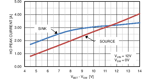
Figure 1. HO Peak Current vs VBST - VSW
LM5122 TC Deadtime vs Vvcc.png
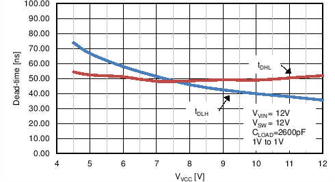
Figure 3. Dead Time vs VVCC
LM5122 TC Deadtime vs vsw.png
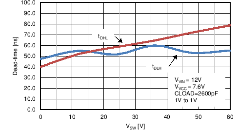
Figure 5. Dead Time vs VSW
LM5122 TC Vvcc vs Ivcc.png
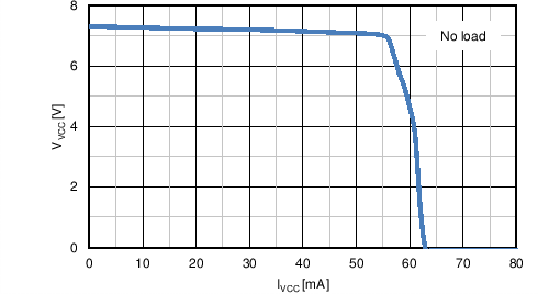
Figure 7. VVCC vs IVCC
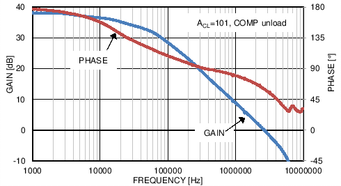
LM5122 TC ErrorAmp_GainPhase.png
Figure 9. Error Amplifier Gain and Phase
vs Frequency
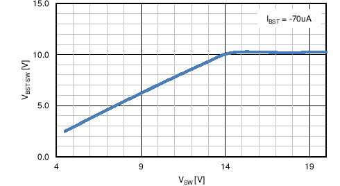
LM5122 TC Vbst-sw vs Vsw.png
Figure 11. VBST-SW vs VSW
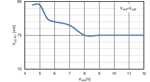
LM5122 TC Vcsth1 vs Vvin.png
Figure 13. VCS-TH1 vs VVIN
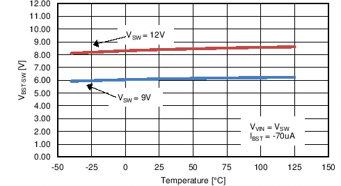
LM5122 TC Vbst-sw vs temp.png
Figure 15. VBST-SW vs Temperature
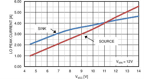
LM5122 TC LO peak current.png
Figure 2. LO Peak Current vs VVCC
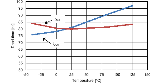
LM5122 TC Deadtime vs Temp.png
Figure 4. Dead Time vs Temperature
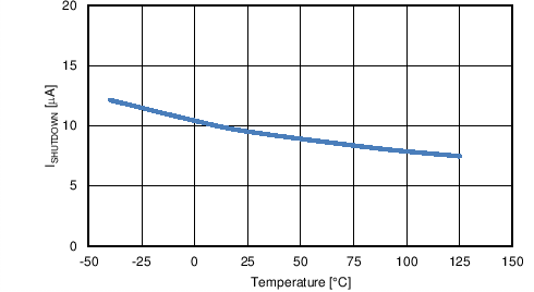
LM5122 TC Ishutdown vs temp.png
Figure 6. ISHUTDOWN vs Temperature
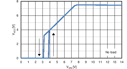
LM5122 TC VCC vs VVIN.png
Figure 8. VVCC vs VVIN
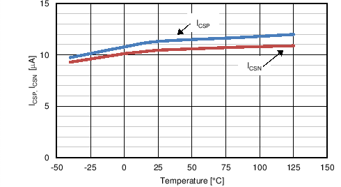
LM5122 TC ICSP ICSN temp.png
Figure 10. ICSP, ICSN vs Temperature
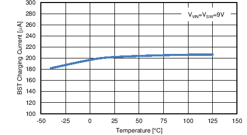
LM5122 TC Ibst vs Temp.png
Figure 12. IBST vs Temperature
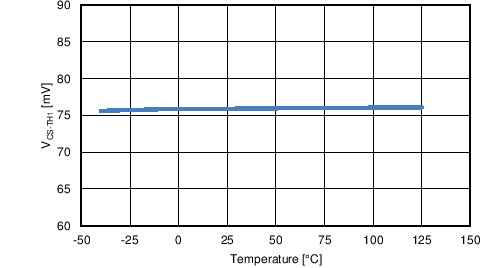
LM5122 TC Vcsth vs temp.png
Figure 14. VCS-TH1 vs Temperature