SNVSB54A May 2018 – November 2018 LM5122ZA
PRODUCTION DATA.
- 1 Features
- 2 Applications
- 3 Description
- 4 Revision History
- 5 Pin Configuration and Functions
- 6 Specifications
-
7 Detailed Description
- 7.1 Overview
- 7.2 Functional Block Diagram
- 7.3
Feature Description
- 7.3.1 Undervoltage Lockout (UVLO)
- 7.3.2 High-Voltage VCC Regulator
- 7.3.3 Oscillator
- 7.3.4 Slope Compensation
- 7.3.5 Error Amplifier
- 7.3.6 PWM Comparator
- 7.3.7 Soft Start
- 7.3.8 HO and LO Drivers
- 7.3.9 Bypass Operation (VOUT = VIN)
- 7.3.10 Cycle-by-Cycle Current Limit
- 7.3.11 Clock Synchronization
- 7.3.12 Maximum Duty Cycle
- 7.3.13 Thermal Protection
- 7.4 Device Functional Modes
-
8 Application and Implementation
- 8.1
Application Information
- 8.1.1 Feedback Compensation
- 8.1.2 Sub-Harmonic Oscillation
- 8.1.3 Interleaved Boost Configuration
- 8.1.4 DCR Sensing
- 8.1.5 Output Overvoltage Protection
- 8.1.6 SEPIC Converter Simplified Schematic
- 8.1.7 Non-Isolated Synchronous Flyback Converter Simplified Schematic
- 8.1.8 Negative to Positive Conversion
- 8.2
Typical Application
- 8.2.1 Design Requirements
- 8.2.2
Detailed Design Procedure
- 8.2.2.1 Timing Resistor RT
- 8.2.2.2 UVLO Divider RUV2, RUV1
- 8.2.2.3 Input Inductor LIN
- 8.2.2.4 Current Sense Resistor RS
- 8.2.2.5 Current Sense Filter RCSFP, RCSFN, CCS
- 8.2.2.6 Slope Compensation Resistor RSLOPE
- 8.2.2.7 Output Capacitor COUT
- 8.2.2.8 Input Capacitor CIN
- 8.2.2.9 VIN Filter RVIN, CVIN
- 8.2.2.10 Bootstrap Capacitor CBST and Boost Diode DBST
- 8.2.2.11 VCC Capacitor CVCC
- 8.2.2.12 Output Voltage Divider RFB1, RFB2
- 8.2.2.13 Soft-Start Capacitor CSS
- 8.2.2.14 Restart Capacitor CRES
- 8.2.2.15 Low-Side Power Switch QL
- 8.2.2.16 High-Side Power Switch QH and Additional Parallel Schottky Diode
- 8.2.2.17 Snubber Components
- 8.2.2.18 Loop Compensation Components CCOMP, RCOMP, CHF
- 8.2.3 Application Curves
- 8.1
Application Information
- 9 Power Supply Recommendations
- 10Layout
- 11Device and Documentation Support
- 12Mechanical, Packaging, and Orderable Information
Package Options
Refer to the PDF data sheet for device specific package drawings
Mechanical Data (Package|Pins)
- PWP|24
Thermal pad, mechanical data (Package|Pins)
Orderable Information
8.1.3 Interleaved Boost Configuration
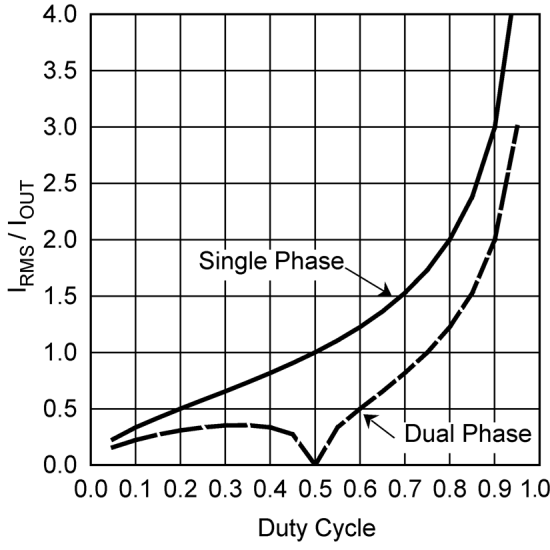
Interleaved operation offers many advantages in single output, high current applications such as higher efficiency, lower component stresses and reduced input and output ripple. For dual phase interleaved operation, the output power path is split reducing the input current in each phase by one-half. Ripple currents in the input and output capacitors are reduced significantly since each channel operates 180 degrees out of phase from the other. Shown in Figure 30 is a normalized (IRMS / IOUT) output capacitor ripple current vs duty cycle for both a single phase and dual phase boost converter, where IRMS is the output current ripple RMS.
 Figure 30. Normalized Output Capacitor RMS Ripple Current
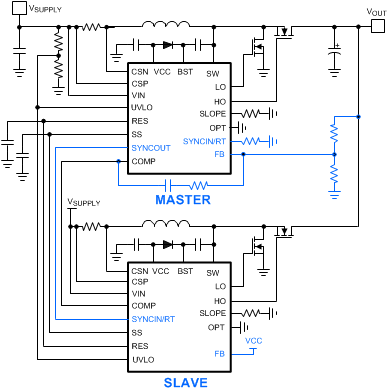
 To configure for dual phase interleaved operation, configure one device as a master and configure the other device in slave mode by connecting FB to VCC. Also connect COMP, UVLO, RES, SS and SYNCOUT on the master side to COMP, UVLO, RES, SS and SYNCIN on slave side, respectively. The compensation network is connected between master FB and the common COMP connection. The output capacitors of the two power stages are connected together at the common output.
 Figure 31. Dual Phase Interleaved Boost Configuration
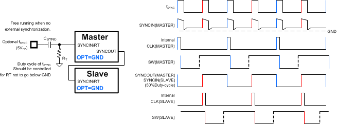
 Shown in Figure 32 is a dual phase timing diagram. The 180° phase shift is realized by connecting SYNCOUT on the master side to the SYNCIN on the slave side.
 Figure 32. Dual Phase Configuration and Timing Diagram
 Each channel is synchronized by an individual external clock in Figure 33. The SYNCOUT pin is used in Figure 34 requiring only one external clock source. A 50% duty cycle of external synchronization pulse should be always provided with this daisy chain configuration.
Current sharing between phases is achieved by sharing one error amplifier output of the master controller with the 3 slave controllers. Resistor sensing is a preferred method of current sensing to accurately balance the phase currents.
![LM5122ZA 4-Phase Timing Diagram Individual Clock LM5122ZA 4 Phase Timing Diag [a].gif](/ods/images/SNVSB54A/4 Phase Timing Diag [a].gif) Figure 33. 4-Phase Timing Diagram Individual Clock
Figure 33. 4-Phase Timing Diagram Individual Clock ![LM5122ZA 4-Phase Timing Diagram Daisy Chain LM5122ZA 4 Phase Timing Diag [b].gif](/ods/images/SNVSB54A/4 Phase Timing Diag [b].gif) Figure 34. 4-Phase Timing Diagram Daisy Chain
Figure 34. 4-Phase Timing Diagram Daisy Chain