SNVSB54A May 2018 – November 2018 LM5122ZA
PRODUCTION DATA.
- 1 Features
- 2 Applications
- 3 Description
- 4 Revision History
- 5 Pin Configuration and Functions
- 6 Specifications
-
7 Detailed Description
- 7.1 Overview
- 7.2 Functional Block Diagram
- 7.3
Feature Description
- 7.3.1 Undervoltage Lockout (UVLO)
- 7.3.2 High-Voltage VCC Regulator
- 7.3.3 Oscillator
- 7.3.4 Slope Compensation
- 7.3.5 Error Amplifier
- 7.3.6 PWM Comparator
- 7.3.7 Soft Start
- 7.3.8 HO and LO Drivers
- 7.3.9 Bypass Operation (VOUT = VIN)
- 7.3.10 Cycle-by-Cycle Current Limit
- 7.3.11 Clock Synchronization
- 7.3.12 Maximum Duty Cycle
- 7.3.13 Thermal Protection
- 7.4 Device Functional Modes
-
8 Application and Implementation
- 8.1
Application Information
- 8.1.1 Feedback Compensation
- 8.1.2 Sub-Harmonic Oscillation
- 8.1.3 Interleaved Boost Configuration
- 8.1.4 DCR Sensing
- 8.1.5 Output Overvoltage Protection
- 8.1.6 SEPIC Converter Simplified Schematic
- 8.1.7 Non-Isolated Synchronous Flyback Converter Simplified Schematic
- 8.1.8 Negative to Positive Conversion
- 8.2
Typical Application
- 8.2.1 Design Requirements
- 8.2.2
Detailed Design Procedure
- 8.2.2.1 Timing Resistor RT
- 8.2.2.2 UVLO Divider RUV2, RUV1
- 8.2.2.3 Input Inductor LIN
- 8.2.2.4 Current Sense Resistor RS
- 8.2.2.5 Current Sense Filter RCSFP, RCSFN, CCS
- 8.2.2.6 Slope Compensation Resistor RSLOPE
- 8.2.2.7 Output Capacitor COUT
- 8.2.2.8 Input Capacitor CIN
- 8.2.2.9 VIN Filter RVIN, CVIN
- 8.2.2.10 Bootstrap Capacitor CBST and Boost Diode DBST
- 8.2.2.11 VCC Capacitor CVCC
- 8.2.2.12 Output Voltage Divider RFB1, RFB2
- 8.2.2.13 Soft-Start Capacitor CSS
- 8.2.2.14 Restart Capacitor CRES
- 8.2.2.15 Low-Side Power Switch QL
- 8.2.2.16 High-Side Power Switch QH and Additional Parallel Schottky Diode
- 8.2.2.17 Snubber Components
- 8.2.2.18 Loop Compensation Components CCOMP, RCOMP, CHF
- 8.2.3 Application Curves
- 8.1
Application Information
- 9 Power Supply Recommendations
- 10Layout
- 11Device and Documentation Support
- 12Mechanical, Packaging, and Orderable Information
Package Options
Refer to the PDF data sheet for device specific package drawings
Mechanical Data (Package|Pins)
- PWP|24
Thermal pad, mechanical data (Package|Pins)
Orderable Information
7.3.7 Soft Start
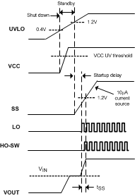
The soft-start feature helps the regulator to gradually reach the steady state operating point, thus reducing start-up stresses and surges. The LM5122ZA regulates the FB pin to the SS pin voltage or the internal 1.2-V reference, whichever is lower. The internal 10-μA soft-start current source gradually increases the voltage on an external soft-start capacitor connected to the SS pin. This results in a gradual rise of the output voltage starting from the input voltage level to the target output voltage. Soft-start time (tSS) which varies by the input supply voltage is calculated from Equation 11.

When the UVLO pin voltage is greater than the 1.2-V UVLO threshold and VCC voltage exceeds the VCC UV threshold, an internal 10-μA soft-start current source turns on. At the beginning of this soft-start sequence, allow VSS to fall down below 25 mV using the internal SS pulldown switch. The SS pin can be pulled down by external switch to stop switching, but pulling up to enable switching is not allowed. The start-up delay (see Figure 22) must be long enough for high-side boot capacitor to be fully charged up by internal BST charge pump.
The value of CSS must be large enough to charge the output capacitor during soft-start time.

 Figure 22. Startup Sequence