SLVSGN5 October 2022 LM51231-Q1
PRODUCTION DATA
- 1 Features
- 2 Applications
- 3 Description
- 4 Revision History
- 5 Pin Configuration and Functions
- 6 Specifications
-
7 Detailed Description
- 7.1 Overview
- 7.2 Functional Block Diagram
- 7.3
Feature Description
- 7.3.1 Device Enable/Disable (EN, VH Pin)
- 7.3.2 High Voltage VCC Regulator (BIAS, VCC Pin)
- 7.3.3 Light Load Switching Mode Selection (MODE Pin)
- 7.3.4 VOUT Range Selection (RANGE Pin)
- 7.3.5 Line Undervoltage Lockout (UVLO Pin)
- 7.3.6 Fast Restart using VCC HOLD (VH Pin)
- 7.3.7 Adjustable Output Regulation Target (VOUT, TRK, VREF Pin)
- 7.3.8 Overvoltage Protection (VOUT Pin)
- 7.3.9 Power Good Indicator (PGOOD Pin)
- 7.3.10 Dynamically Programmable Switching Frequency (RT)
- 7.3.11 External Clock Synchronization (SYNC Pin)
- 7.3.12 Programmable Spread Spectrum (DITHER Pin)
- 7.3.13 Programmable Soft-start (SS Pin)
- 7.3.14 Wide Bandwidth Transconductance Error Amplifier and PWM (TRK, COMP Pin)
- 7.3.15 Current Sensing and Slope Compensation (CSP, CSN Pin)
- 7.3.16 Constant Peak Current Limit (CSP, CSN Pin)
- 7.3.17 Maximum Duty Cycle and Minimum Controllable On-time Limits
- 7.3.18 MOSFET Drivers, Integrated Boot Diode, and Hiccup Mode Fault Protection (LO, HO, HB Pin)
- 7.3.19 Thermal Shutdown Protection
- 7.4 Device Functional Modes
- 8 Application and Implementation
- 9 Device and Documentation Support
- 10Mechanical, Packaging, and Orderable Information
Package Options
Mechanical Data (Package|Pins)
- RGR|20
Thermal pad, mechanical data (Package|Pins)
- RGR|20
Orderable Information
3 Description
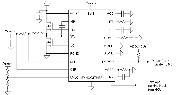
The LM51231-Q1 device is a wide input range synchronous boost controller that employs peak current mode control. The device's wide input range supports automotive cold-crank and load dump. The minimum input voltage can be as low as 0.8 V when BIAS is equal to or greater than 3.8 V. The output voltage can be dynamically programmed by using the tracking function. Bypass mode operation is automatically entered when VSUPPLY > VLOAD, eliminating the body diode drop of the high-side MOSFET. The switching frequency is dynamically programmed with an external resistor from 100 kHz to 2.2 MHz. Switching at 2.2 MHz minimizes AM band interference and allows a small solution size and fast transient response.
The device has built-in protection features such as peak current limit, which is constant over VSUPPLY, overvoltage protection, and thermal shutdown. External clock synchronization, programmable spread spectrum modulation, and a lead-less package with minimal parasitic, help to reduce EMI and avoid cross talk. Additional features include line UVLO, FPWM, diode emulation, DCR inductor current sensing, programmable soft start, and a power-good indicator
| PART NUMBER | PACKAGE(1) | BODY SIZE (NOM) |
|---|---|---|
| LM51231-Q1 | QFN (20) | 3.5 mm x 3.5 mm |
 Typical
Application