SNVSC77 December 2024 LM5125-Q1
ADVANCE INFORMATION
- 1
- 1 Features
- 2 Applications
- 3 Description
- 4 Pin Configuration and Functions
- 5 Specifications
-
6 Detailed Description
- 6.1 Overview
- 6.2 Functional Block Diagram
- 6.3
Feature Description
- 6.3.1 Device Configuration (CFG0-pin, CFG1-pin, CFG2-pin)
- 6.3.2 Switching Frequency and Synchronization (SYNCIN)
- 6.3.3 Dual Random Spread Spectrum (DRSS)
- 6.3.4 Operation Modes (BYPASS, DEM, FPWM)
- 6.3.5 Dual- and Multi-phase Operation
- 6.3.6 BIAS (BIAS-pin)
- 6.3.7 Soft Start (SS-pin)
- 6.3.8 VOUT Programming (VOUT, ATRK, DTRK)
- 6.3.9 Protections
- 6.3.10 VOUT Overvoltage Protection (OVP)
- 6.3.11 Thermal Shutdown (TSD)
- 6.3.12 Power-Good Indicator (PGOOD-pin)
- 6.3.13 Current Sensing, Peak Current Limit, and Slope Compensation (CSP1, CSP2, CSN1, CSN2)
- 6.3.14 Current Sense Programming (CSP1, CSP2, CSN1, CSN2)
- 6.3.15 Input Current Limit and Monitoring (ILIM, IMON, DLY)
- 6.3.16 Signal Deglitch Overview
- 6.3.17 MOSFET Drivers, Integrated Boot Diode, and Hiccup Mode Fault Protection (LOx, HOx, HBx-pin)
- 6.4 Device Functional Modes
-
7 Application and Implementation
- 7.1 Application Information
- 7.2
Typical Application
- 7.2.1 Application
- 7.2.2 Design Requirements
- 7.2.3
Detailed Design Procedure
- 7.2.3.1 Determine the Total Phase Number
- 7.2.3.2 Determining the Duty Cycle
- 7.2.3.3 Timing Resistor RT
- 7.2.3.4 Inductor Selection Lm
- 7.2.3.5 Current Sense Resistor Rcs
- 7.2.3.6 Current Sense Filter RCSFP, RCSFN, CCS
- 7.2.3.7 Low-Side Power Switch QL
- 7.2.3.8 High-Side Power Switch QH and Additional Parallel Schottky Diode
- 7.2.3.9 Snubber Components
- 7.2.3.10 Vout Programming
- 7.2.3.11 Input Current Limit (ILIM/IMON)
- 7.2.3.12 UVLO Divider
- 7.2.3.13 Soft Start
- 7.2.3.14 CFG Settings
- 7.2.3.15 Output Capacitor Cout
- 7.2.3.16 Input Capacitor Cin
- 7.2.3.17 Bootstrap Capacitor
- 7.2.3.18 VCC Capacitor CVCC
- 7.2.3.19 BIAS Capacitor
- 7.2.3.20 VOUT Capacitor
- 7.2.3.21 Loop Compensation
- 7.2.4 Application Curves
- 7.3 Power Supply Recommendations
- 7.4 Layout
- 8 Device and Documentation Support
- 9 Revision History
- 10Mechanical, Packaging, and Orderable Information
Package Options
Mechanical Data (Package|Pins)
- RHB|32
Thermal pad, mechanical data (Package|Pins)
6.3.3 Dual Random Spread Spectrum (DRSS)
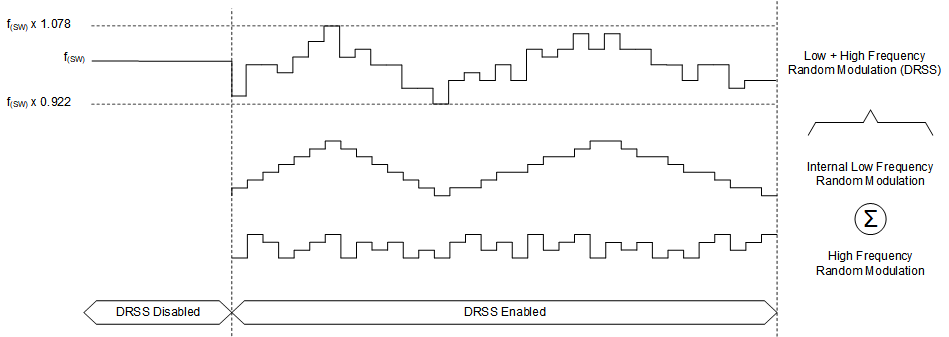
The device provides a digital spread spectrum, which reduces the EMI of the power supply over a wide frequency range. This function can be enabled by the CFG1-pin. When the spread spectrum is enabled, the internal modulator dithers the internal clock. When the device is configured to use an external clock applied at the SYNCIN-pin, the internal spread spectrum is disabled. DRSS combines a low frequency triangular modulation profile with a high frequency cycle-by-cycle random modulation profile. The low frequency triangular modulation improves performance in lower radio frequency bands (for example AM band), while the high frequency random modulation improves performance in higher radio frequency bands (for example FM band). In addition, the frequency of the triangular modulation is further modulated randomly to reduce the likelihood of any audible tones. To minimize output voltage ripple caused by spread spectrum, duty cycle is modified on a cycle-by-cycle basis to maintain a nearly constant duty cycle when dithering is enabled.
In dual device configuration DRSS is damped in the 2nd device for switching frequencies < 220kHz.
 Figure 6-2 Dual Random Spread
Spectrum