SNVS808C May 2012 – Februrary 2016 LM5134
PRODUCTION DATA.
- 1 Features
- 2 Applications
- 3 Description
- 4 Revision History
- 5 Pin Configuration and Functions
- 6 Specifications
- 7 Detailed Description
- 8 Application and Implementation
- 9 Power Supply Recommendations
- 10Layout
- 11Device and Documentation Support
- 12Mechanical, Packaging, and Orderable Information
Package Options
Mechanical Data (Package|Pins)
Thermal pad, mechanical data (Package|Pins)
Orderable Information
7 Detailed Description
7.1 Overview
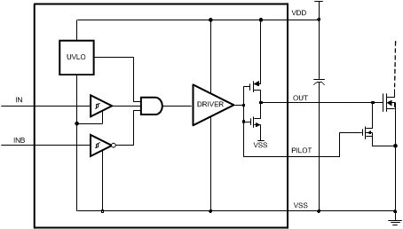
The LM5134 is a single low-side gate driver with one main output, OUT, and a complementary output PILOT. The OUT pin has high 7.6-A and 4.5-A peak sink and source current and can be used to drive large power MOSFETs or multiple MOSFETs in parallel. The PILOT pin has 820-mA and 660-mA peak sink and source current, and is intended to drive an external turnoff MOSFET, as shown in Functional Block Diagram. The external turnoff FET can be placed close to the power MOSFETs to minimize the loop inductance, and therefore helps eliminate stray inductance induced oscillations or undesired turnon. This feature also provides the flexibility to adjust turnon and turnoff speed independently.
7.2 Functional Block Diagram

7.3 Feature Description
When using the external turnoff switch, it is important to prevent the potential shoot-through between the external turnoff switch and the LM5134 internal pullup switch. The propagation delay, TPD-ON and TPD-OFF, has been implemented in the LM5134 between the PILOT and the OUT pins, as depicted in the timing diagram. The turnon delay TPD-ON is designed to be shorter than the turnoff delay TPD-OFF because the rising time of the external turnoff switch can attribute to the additional delay time. It is also desirable to minimize TPD-ON to favor the fast turnoff of the power MOSFET.
The LM5134 offers both inverting and noninverting inputs to satisfy requirements for inverting and non-inverting gate drive signals in a single device type. Inputs of the LM5134 are TTL and CMOS Logic compatible and can withstand input voltages up to 14 V regardless of the VDD voltage. This allows inputs of the LM5134 to be connected directly to most PWM controllers.
The LM5134 includes an Undervoltage Lockout (UVLO) circuit. When the VDD voltage is below the UVLO threshold voltage, the IN and INB inputs are ignored, and if there is sufficient VDD voltage, the OUT is pulled low. In addition, the LM5134 has an internal PNP transistor in parallel with the output NMOS. Under the UVLO condition, the PNP transistor will be on and clamp the OUT voltage below 1 V. This feature ensures the OUT remains low even with insufficient VDD voltage.