SNVS808C May 2012 – Februrary 2016 LM5134
PRODUCTION DATA.
- 1 Features
- 2 Applications
- 3 Description
- 4 Revision History
- 5 Pin Configuration and Functions
- 6 Specifications
- 7 Detailed Description
- 8 Application and Implementation
- 9 Power Supply Recommendations
- 10Layout
- 11Device and Documentation Support
- 12Mechanical, Packaging, and Orderable Information
Package Options
Mechanical Data (Package|Pins)
Thermal pad, mechanical data (Package|Pins)
Orderable Information
10 Layout
10.1 Layout Guidelines
Attention must be given to board layout when using LM5134. Some important considerations include:
- The first priority in designing the layout of the driver is to confine the high peak currents that charge and discharge the FETs gate into a minimal physical area. This will decrease the loop inductance and minimize noise issues on the gate.
- To reduce the loop inductance, the driver should be placed as close as possible to the FETs. The gate trace to and from the FETs are recommended to be placed closely side by side, or directly on top of one another.
- The parasitic source inductance, along with the gate capacitor and the driver pulldown path, can form a LCR resonant tank, resulting in gate voltage oscillations. An optional resistor or ferrite bead can be used to damp the ringing.
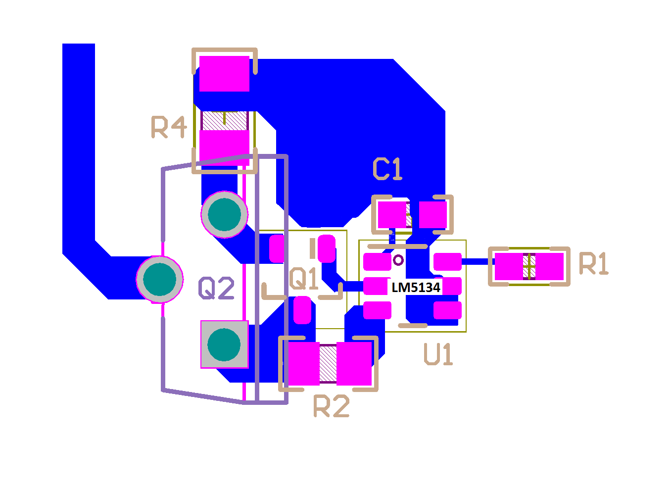
10.2 Layout Example
 Figure 27. LM5134 Layout Example
10.3 Power Dissipation
It is important to keep the power consumption of the driver below the maximum power dissipation limit of the package at the operating temperature. The total power dissipation of the LM5134 is the sum of the gate charge losses and the losses in the driver due to the internal CMOS stages used to buffer the output as well as the power losses associated with the quiescent current.
The gate charge losses include the power MOSFET gate charge losses as well as the PILOT FET gate charge losses and can be calculated as follows:
Or
where
- Fsw is switching frequency
- Qgo is the total input gate charge of the power MOSFET
- Qgp is the total input gate charge of the PILOT MOSFET
Co and Cp are the load capacitance at OUT and PILOT outputs respectively. It should be noted that due to the use of an external turnoff switch, part of the gate charge losses are dissipated in the external turnoff switch. Therefore, the actual gate charge losses dissipated in the LM5134 is less than predicted by the above expressions. However, they are a good conservative design estimate.
The power dissipation associated with the internal circuit operation of the driver can be estimated with the characterization curves of the LM5134. For a given ambient temperature, the maximum allowable power losses of the IC can be defined using Equation 4.
where
- P is the total power dissipation of the driver