SNVSCU2A August 2024 – August 2024 LM5137-Q1
ADVANCE INFORMATION
- 1
- 1 Features
- 2 Applications
- 3 Description
- 4 Device Comparison Table
- 5 Pin Configuration and Functions
- 6 Specifications
-
7 Detailed Description
- 7.1 Overview
- 7.2 Functional Block Diagram
- 7.3
Feature Description
- 7.3.1 Input Voltage Range (VIN)
- 7.3.2 Bias Supply Regulator (VCC, BIAS1/VOUT1, VDDA)
- 7.3.3 Precision Enable (EN1, EN2)
- 7.3.4 Switching Frequency (RT)
- 7.3.5 Pulse Frequency Modulation and Synchronization (PFM/SYNC)
- 7.3.6 Synchronization Out (SYNCOUT)
- 7.3.7 Dual Random Spread Spectrum (DRSS)
- 7.3.8 Configurable Soft Start (RSS)
- 7.3.9 Output Voltage Setpoints (FB1, FB2)
- 7.3.10 Minimum Controllable On-Time
- 7.3.11 Error Amplifier and PWM Comparator (FB1, FB2, COMP1, COMP2)
- 7.3.12 Inductor Current Sense (ISNS1+, BIAS1/VOUT1, ISNS2+, VOUT2)
- 7.3.13 MOSFET Gate Drivers (HO1, HO2, LO1, LO2)
- 7.3.14 Output Configurations (CNFG)
- 7.4 Device Functional Modes
-
8 Application and Implementation
- 8.1 Application Information
- 8.2
Typical Applications
- 8.2.1
Design 1 – Dual 5V and 3.3V, 20A Buck Regulator for 12V
Automotive Battery Applications
- 8.2.1.1 Design Requirements
- 8.2.1.2
Detailed Design Procedure
- 8.2.1.2.1 Custom Design With WEBENCH® Tools
- 8.2.1.2.2 Custom Design With Excel Quickstart Tool
- 8.2.1.2.3 Inductor Calculations
- 8.2.1.2.4 Shunt Resistors
- 8.2.1.2.5 Ceramic Output Capacitors
- 8.2.1.2.6 Ceramic Input Capacitors
- 8.2.1.2.7 Feedback Resistors
- 8.2.1.2.8 Input Voltage UVLO Resistors
- 8.2.1.2.9 Compensation Components
- 8.2.1.3 Application Curves
- 8.2.2 Design 2 – Two-Phase, Single-Output Buck Regulator for Automotive ADAS Applications
- 8.2.3 Design 3 – 12V, 20A, 400kHz, Two-Phase Buck Regulator for 48V Automotive Applications
- 8.2.1
Design 1 – Dual 5V and 3.3V, 20A Buck Regulator for 12V
Automotive Battery Applications
- 8.3 Power Supply Recommendations
- 8.4 Layout
- 9 Device and Documentation Support
- 10Revision History
- 11Mechanical, Packaging, and Orderable Information
Package Options
Mechanical Data (Package|Pins)
- RHA|36
Thermal pad, mechanical data (Package|Pins)
Orderable Information
7.3.7 Dual Random Spread Spectrum (DRSS)
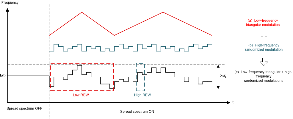
The LM5137-Q1 provides a digital spread spectrum, which reduces the EMI signature of the switching regulator over a wide frequency range. As shown in Figure 7-3, DRSS combines a low-frequency triangular modulation profile with a high frequency cycle-by-cycle random modulation profile. The low-frequency modulation improves performance in lower radio-frequency bands, while the high-frequency random modulation improves performance in higher radio-frequency bands.
Spread spectrum functions by converting a narrowband signal into a wideband signal that spreads the energy over multiple frequencies. Because industry standards require different EMI receiver resolution bandwidth (RBW) settings for different frequency bands, the RBW has an impact on the spread spectrum performance. For example, the RBW setting in an EMI receiver for CISPR 25 in the frequency band from 150kHz to 30MHz is 9kHz. For frequencies greater than 30MHz, the RBW is 120kHz. DRSS is able to simultaneously improve the EMI performance with low and high RBWs with the low-frequency triangular and high-frequency cycle-by-cycle random modulation profiles, respectively. DRSS can reduce conducted emissions by 15dBμV in the CISPR 25 low-frequency band (150kHz to 30MHz) and 5dBμV in the high-frequency band (30MHz to 108MHz). Applying an external clock signal to the PFM/SYNCIN pin disables DRSS. See Table 7-3 to configure the LM5137-Q1 using a resistor from CNFG to AGND.
| RCNFG | PRIMARY / SECONDARY | DRSS | INDEPENDENT OR INTERLEAVED |
|---|---|---|---|
| 10kΩ | Primary | Disabled | Independent |
| 19.1kΩ | Primary | ±5% | Independent |
| 29.4kΩ | Primary | ±10% | Independent |
| 41.2kΩ | Primary | Disabled | Interleaved |
| 54.9kΩ | Primary | ±5% | Interleaved |
| 71.5kΩ | Primary | ±10% | Interleaved |
| 90.9kΩ | Secondary | N/A | Interleaved |
 Figure 7-3 DRSS Implementation