SNVSB29C October 2018 – June 2021 LM5143-Q1
PRODUCTION DATA
- 1 Features
- 2 Applications
- 3 Description
- 4 Revision History
- 5 Description (continued)
- 6 Pin Configuration and Functions
- 7 Specifications
-
8 Detailed Description
- 8.1 Overview
- 8.2 Functional Block Diagram
- 8.3
Feature Description
- 8.3.1 Input Voltage Range (VIN)
- 8.3.2 High-Voltage Bias Supply Regulator (VCC, VCCX, VDDA)
- 8.3.3 Enable (EN1, EN2)
- 8.3.4 Power Good Monitor (PG1, PG2)
- 8.3.5 Switching Frequency (RT)
- 8.3.6 Clock Synchronization (DEMB)
- 8.3.7 Synchronization Out (SYNCOUT)
- 8.3.8 Spread Spectrum Frequency Modulation (DITH)
- 8.3.9 Configurable Soft Start (SS1, SS2)
- 8.3.10 Output Voltage Setpoint (FB1, FB2)
- 8.3.11 Minimum Controllable On-Time
- 8.3.12 Error Amplifier and PWM Comparator (FB1, FB2, COMP1, COMP2)
- 8.3.13 Slope Compensation
- 8.3.14 Inductor Current Sense (CS1, VOUT1, CS2, VOUT2)
- 8.3.15 Hiccup Mode Current Limiting (RES)
- 8.3.16 High-Side and Low-Side Gate Drivers (HO1/2, LO1/2, HOL1/2, LOL1/2)
- 8.3.17 Output Configurations (MODE, FB2)
- 8.4 Device Functional Modes
-
9 Application and Implementation
- 9.1 Application Information
- 9.2 Typical Applications
- 10Power Supply Recommendations
- 11Layout
- 12Device and Documentation Support
- 13Mechanical, Packaging, and Orderable Information
Package Options
Mechanical Data (Package|Pins)
- RWG|40
Thermal pad, mechanical data (Package|Pins)
Orderable Information
8.3.15 Hiccup Mode Current Limiting (RES)
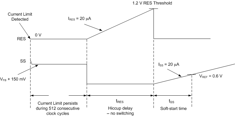
The LM5143-Q1 includes an optional hiccup mode protection function that is enabled when a capacitor is connected to the RES pin. In normal operation, the RES capacitor is discharged to ground. If 512 cycles of cycle-by-cycle current limiting occurs, SS is pulled low and the HO and LO outputs are disabled (see Figure 8-6). A 20-μA current source begins to charge the RES capacitor. When the RES voltage increases to 1.2 V, RES is pulled low and the SS capacitor begins to charge. The 512-cycle hiccup counter is reset if four consecutive switching cycles occur without exceeding the current limit threshold. Separate hiccup counters are provided for each channel, but the RES pin is shared by both channels. One channel can be in hiccup protection while the other operates normally. In the event that both channels are in an overcurrent condition triggering hiccup protection, the last hiccup counter to expire pulls RES low and starts the RES capacitor charging cycle. Both channels then restart together when VRES = 1.2 V. If RES is connected to VDDA at power up, the hiccup function is disabled for both channels.
 Figure 8-6 Hiccup Mode Timing Diagram
Use Equation 13 to calculate the RES capacitance.

where
- tRES is the specified hiccup delay as shown in Figure 8-6