SNVSB29C October 2018 – June 2021 LM5143-Q1
PRODUCTION DATA
- 1 Features
- 2 Applications
- 3 Description
- 4 Revision History
- 5 Description (continued)
- 6 Pin Configuration and Functions
- 7 Specifications
-
8 Detailed Description
- 8.1 Overview
- 8.2 Functional Block Diagram
- 8.3
Feature Description
- 8.3.1 Input Voltage Range (VIN)
- 8.3.2 High-Voltage Bias Supply Regulator (VCC, VCCX, VDDA)
- 8.3.3 Enable (EN1, EN2)
- 8.3.4 Power Good Monitor (PG1, PG2)
- 8.3.5 Switching Frequency (RT)
- 8.3.6 Clock Synchronization (DEMB)
- 8.3.7 Synchronization Out (SYNCOUT)
- 8.3.8 Spread Spectrum Frequency Modulation (DITH)
- 8.3.9 Configurable Soft Start (SS1, SS2)
- 8.3.10 Output Voltage Setpoint (FB1, FB2)
- 8.3.11 Minimum Controllable On-Time
- 8.3.12 Error Amplifier and PWM Comparator (FB1, FB2, COMP1, COMP2)
- 8.3.13 Slope Compensation
- 8.3.14 Inductor Current Sense (CS1, VOUT1, CS2, VOUT2)
- 8.3.15 Hiccup Mode Current Limiting (RES)
- 8.3.16 High-Side and Low-Side Gate Drivers (HO1/2, LO1/2, HOL1/2, LOL1/2)
- 8.3.17 Output Configurations (MODE, FB2)
- 8.4 Device Functional Modes
-
9 Application and Implementation
- 9.1 Application Information
- 9.2 Typical Applications
- 10Power Supply Recommendations
- 11Layout
- 12Device and Documentation Support
- 13Mechanical, Packaging, and Orderable Information
Package Options
Mechanical Data (Package|Pins)
- RWG|40
Thermal pad, mechanical data (Package|Pins)
Orderable Information
8.3.1 Input Voltage Range (VIN)
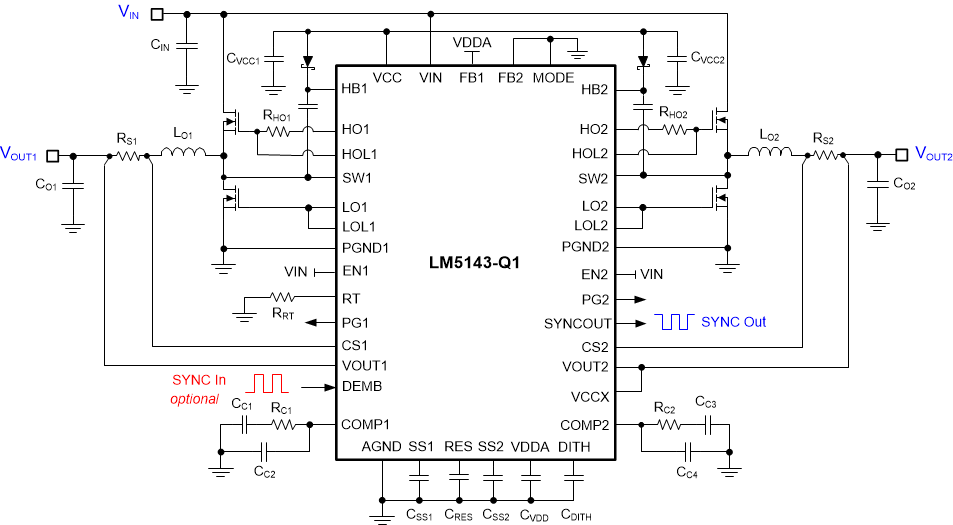
The LM5143-Q1 operational input voltage range is from 3.5 V to 65 V. The device is intended for step-down conversions from 12-V, 24-V, and 48-Vautomotive supply rails. The application circuit in Figure 8-1 shows all the necessary components to implement an LM5143-Q1 based wide-VIN dual-output step-down regulator using a single supply. The LM5143-Q1 uses an internal LDO subregulator to provide a 5-V VCC bias rail for the gate drive and control circuits (assuming the input voltage is higher than 5 V plus the necessary subregulator dropout specification).
 Figure 8-1 Dual-Output Regulator Schematic Diagram With Input Voltage Range of 3.5 V to 65 V
In high input voltage applications, make sure the VIN and SW pins do not exceed their absolute maximum voltage rating of 70 V during line or load transient events. Voltage excursions that exceed the Absolute Maximum Ratings can damage the IC. Proceed carefully during PCB board layout and use high-quality input bypass capacitors to minimize voltage overshoot and ringing.