SNVSBU9A
June 2021 – June 2021
LM5145-Q1
PRODUCTION DATA
1
Features
2
Applications
3
Description
4
Revision History
5
Description (continued)
6
Pin Configuration and Functions
6.1
Wettable Flanks
7
Specifications
7.1
Absolute Maximum Ratings
7.2
ESD Ratings
7.3
Recommended Operating Conditions
7.4
Thermal Information
7.5
Electrical Characteristics
7.6
Switching Characteristics
7.7
Typical Characteristics
8
Detailed Description
8.1
Overview
8.2
Functional Block Diagram
8.3
Feature Description
8.3.1
Input Range (VIN)
8.3.2
Output Voltage Setpoint and Accuracy (FB)
8.3.3
High-Voltage Bias Supply Regulator (VCC)
8.3.4
Precision Enable (EN/UVLO)
8.3.5
Power Good Monitor (PGOOD)
8.3.6
Switching Frequency (RT, SYNCIN)
8.3.6.1
Frequency Adjust
8.3.6.2
Clock Synchronization
8.3.7
Configurable Soft Start (SS/TRK)
8.3.7.1
Tracking
8.3.8
Voltage-Mode Control (COMP)
8.3.9
Gate Drivers (LO, HO)
8.3.10
Current Sensing and Overcurrent Protection (ILIM)
8.3.11
OCP Duty Cycle Limiter
8.4
Device Functional Modes
8.4.1
Shutdown Mode
8.4.2
Standby Mode
8.4.3
Active Mode
8.4.4
Diode Emulation Mode
8.4.5
Thermal Shutdown
9
Application and Implementation
9.1
Application Information
9.1.1
Design and Implementation
9.1.2
Power Train Components
9.1.2.1
Inductor
9.1.2.2
Output Capacitors
9.1.2.3
Input Capacitors
9.1.2.4
Power MOSFETs
9.1.3
Control Loop Compensation
9.1.4
EMI Filter Design
9.2
Typical Applications
9.2.1
Design 1 – 12-A High-Efficiency Synchronous Buck DC/DC Regulator for Automotive Applications
9.2.1.1
Design Requirements
9.2.1.2
Detailed Design Procedure
9.2.1.2.1
Custom Design With WEBENCH® Tools
9.2.1.2.2
Custom Design With Excel Quickstart Tool
9.2.1.3
Application Curves
9.2.2
Design 2 – High Density, 12-V, 8-A Rail From 48-V Automotive Battery Power
9.2.2.1
Design Requirements
9.2.2.2
Detailed Design Procedure
9.2.2.3
Application Curves
10
Power Supply Recommendations
11
Layout
11.1
Layout Guidelines
11.1.1
Power Stage Layout
11.1.2
Gate Drive Layout
11.1.3
PWM Controller Layout
11.1.4
Thermal Design and Layout
11.1.5
Ground Plane Design
11.2
Layout Example
12
Device and Documentation Support
12.1
Device Support
12.1.1
Third-Party Products Disclaimer
12.1.2
Development Support
12.1.2.1
Custom Design With WEBENCH® Tools
12.2
Documentation Support
12.2.1
Related Documentation
12.2.1.1
PCB Layout Resources
12.2.1.2
Thermal Design Resources
12.3
Receiving Notification of Documentation Updates
12.4
Support Resources
12.5
Trademarks
12.6
Electrostatic Discharge Caution
12.7
Glossary
13
Mechanical, Packaging, and Orderable Information
Package Options
Mechanical Data (Package|Pins)
RGY|20
MPQF116H
Thermal pad, mechanical data (Package|Pins)
RGY|20
QFND600
Orderable Information
snvsbu9a_oa
snvsbu9a_pm
9.2.1.3
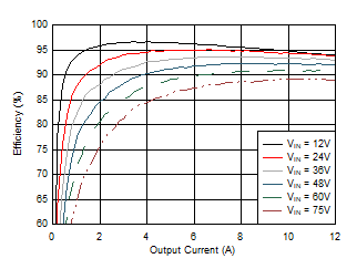
Application Curves
Figure 9-6
Efficiency and Power Loss vs I
OUT
and V
IN
V
IN
step to 48 V
0.8-Ω Load
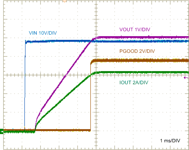
Figure 9-8
Start-Up, Resistive Load
V
IN
= 48 V
0.8-Ω Load
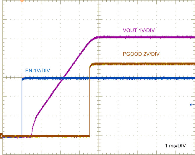
Figure 9-10
ENABLE ON, Resistive Load
V
IN
= 48 V
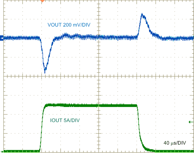
Figure 9-12
Load Transient Response, 0 A to 12 A to 0 A
I
OUT
= 6 A
Figure 9-14
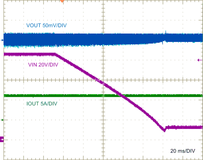
Line Transient Response, 85 V to 12 V
V
IN
= 48 V
I
OUT
= 6 A
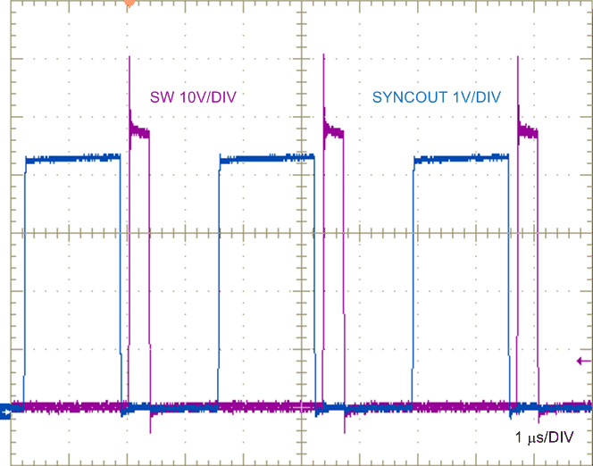
Figure 9-7
SYNCOUT and SW Node Voltages
V
IN
48 V to 6 V
0.8-Ω Load
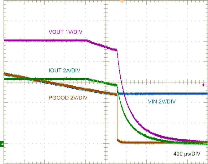
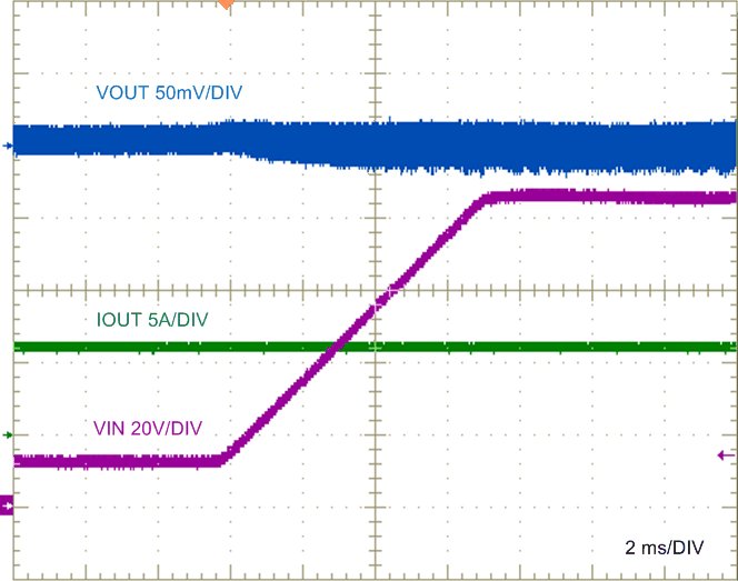
Figure 9-9
Shutdown Through UVLO
V
IN
= 48 V
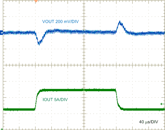
Figure 9-11
Load Transient Response, 6 A to 12 A to 6 A
I
OUT
= 6 A
Figure 9-13
Line Transient Response, 12 V to 85 V
V
IN
= 48 V
I
OUT
= 0 A
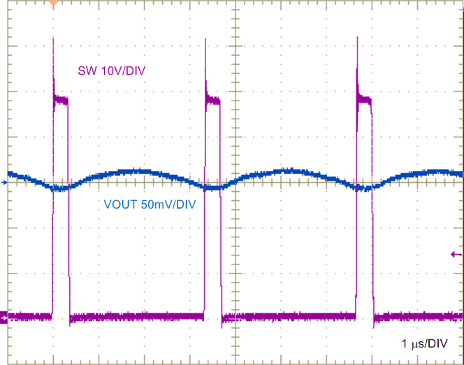
Figure 9-15
SW Node and Output Ripple Voltages