SNVSC01 February 2023 LM5148
PRODUCTION DATA
- 1 Features
- 2 Applications
- 3 Description
- 4 Revision History
- 5 Description (continued)
- 6 Pin Configuration and Functions
- 7 Specifications
-
8 Detailed Description
- 8.1 Overview
- 8.2 Functional Block Diagram
- 8.3
Feature Description
- 8.3.1 Input Voltage Range (VIN)
- 8.3.2 High-Voltage Bias Supply Regulator (VCC, VCCX, VDDA)
- 8.3.3 Precision Enable (EN)
- 8.3.4 Power-Good Monitor (PG)
- 8.3.5 Switching Frequency (RT)
- 8.3.6 Dual Random Spread Spectrum (DRSS)
- 8.3.7 Soft Start
- 8.3.8 Output Voltage Setpoint (FB)
- 8.3.9 Minimum Controllable On Time
- 8.3.10 Error Amplifier and PWM Comparator (FB, EXTCOMP)
- 8.3.11 Slope Compensation
- 8.3.12 Inductor Current Sense (ISNS+, VOUT)
- 8.3.13 Hiccup Mode Current Limiting
- 8.3.14 High-Side and Low-Side Gate Drivers (HO, LO)
- 8.3.15 Output Configurations (CNFG)
- 8.3.16 Single-Output Dual-Phase Operation
- 8.4 Device Functional Modes
-
9 Application and Implementation
- 9.1 Application Information
- 9.2
Typical Applications
- 9.2.1
Design 1 – High Efficiency 2.1-MHz Synchronous
Buck Regulator
- 9.2.1.1 Design Requirements
- 9.2.1.2
Detailed Design Procedure
- 9.2.1.2.1 Custom Design with WEBENCH® Tools
- 9.2.1.2.2 Custom Design with Excel Quickstart Tool
- 9.2.1.2.3 Buck Inductor
- 9.2.1.2.4 Current-Sense Resistance
- 9.2.1.2.5 Output Capacitors
- 9.2.1.2.6 Input Capacitors
- 9.2.1.2.7 Frequency Set Resistor
- 9.2.1.2.8 Feedback Resistors
- 9.2.1.2.9 Compensation Components
- 9.2.1.3 Application Curves
- 9.2.2 Design 2 – High Efficiency 48-V to 12-V 400-kHz Synchronous Buck Regulator
- 9.2.3 Design 3 – High Efficiency 440-kHz Synchronous Buck Regulator
- 9.2.4 Design 4 – Dual-Phase 400-kHz 20-A Synchronous Buck Regulator
- 9.2.1
Design 1 – High Efficiency 2.1-MHz Synchronous
Buck Regulator
- 9.3 Power Supply Recommendations
- 9.4 Layout
- 10Device and Documentation Support
- 11Mechanical, Packaging, and Orderable Information
Package Options
Mechanical Data (Package|Pins)
- RGY|24
Thermal pad, mechanical data (Package|Pins)
- RGY|24
Orderable Information
3 Description
The LM5148 is a 80-V, ultra-low IQ synchronous buck DC/DC controller for high-current, single-output applications. The controller uses a peak current-mode control architecture for easy loop compensation, fast transient response, and excellent load and line regulation. The LM5148 can be set up in idual-phase mode (paralleled output) with accurate current sharing for high-current applications. It can operate at input voltages as low as 3.5 V, at nearly 100% duty cycle if needed.
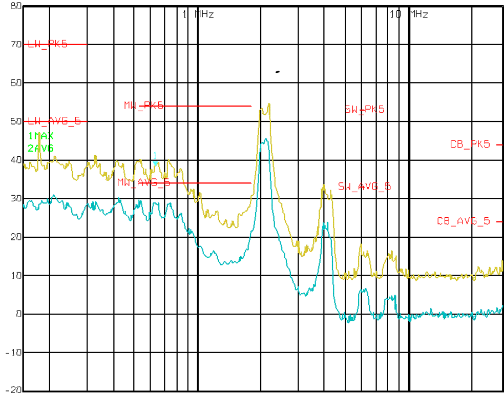
The LM5148 has a unique EMI reduction feature known as dual random spread spectrum (DRSS). Combining low-frequency triangular and high-frequency random modulations mitigates EMI disturbances across lower and higher frequency bands, respectively. This hybrid technique aligns with the multiple resolution bandwidth (RBW) settings specified in industry-standard EMC tests.
| PART NUMBER | PACKAGE(1) | BODY SIZE (NOM) |
|---|---|---|
| LM5148 | RGY (VQFN, 24) | 3.50 mm × 5.50 mm |
 CISPR
25 EMI Performance - 150 kHz to 30 MHz