SNVSBV4A December 2020 – January 2023 LM5149
PRODUCTION DATA
- 1 Features
- 2 Applications
- 3 Description
- 4 Revision History
- 5 Description (continued)
- 6 Pin Configuration and Functions
- 7 Specifications
-
8 Detailed Description
- 8.1 Overview
- 8.2 Functional Block Diagram
- 8.3
Feature Description
- 8.3.1 Input Voltage Range (VIN)
- 8.3.2 High-Voltage Bias Supply Regulator (VCC, VCCX, VDDA)
- 8.3.3 Precision Enable (EN)
- 8.3.4 Power-Good Monitor (PG)
- 8.3.5 Switching Frequency (RT)
- 8.3.6 Active EMI Filter
- 8.3.7 Dual Random Spread Spectrum (DRSS)
- 8.3.8 Soft Start
- 8.3.9 Output Voltage Setpoint (FB)
- 8.3.10 Minimum Controllable On Time
- 8.3.11 Error Amplifier and PWM Comparator (FB, EXTCOMP)
- 8.3.12 Slope Compensation
- 8.3.13 Inductor Current Sense (ISNS+, VOUT)
- 8.3.14 Hiccup Mode Current Limiting
- 8.3.15 High-Side and Low-Side Gate Drivers (HO, LO)
- 8.3.16 Output Configurations (CNFG)
- 8.3.17 Single-Output Dual-Phase Operation
- 8.4 Device Functional Modes
-
9 Application and Implementation
- 9.1 Application Information
- 9.2
Typical Applications
- 9.2.1
Design 1 – High-Efficiency 2.1-MHz Synchronous
Buck Regulator
- 9.2.1.1 Design Requirements
- 9.2.1.2
Detailed Design Procedure
- 9.2.1.2.1 Custom Design With WEBENCH® Tools
- 9.2.1.2.2 Custom Design With Excel Quickstart Tool
- 9.2.1.2.3 Buck Inductor
- 9.2.1.2.4 Current-Sense Resistance
- 9.2.1.2.5 Output Capacitors
- 9.2.1.2.6 Input Capacitors
- 9.2.1.2.7 Frequency Set Resistor
- 9.2.1.2.8 Feedback Resistors
- 9.2.1.2.9 Compensation Components
- 9.2.1.3 Application Curves
- 9.2.2 Design 2 – High Efficiency 48-V to 12-V 400-kHz Synchronous Buck Regulator
- 9.2.3 Design 3 – High Efficiency 440-kHz Synchronous Buck Regulator
- 9.2.4 Design 4 – Dual-Phase 400-kHz 20-A Synchronous Buck Regulator
- 9.2.1
Design 1 – High-Efficiency 2.1-MHz Synchronous
Buck Regulator
- 9.3 Power Supply Recommendations
- 9.4 Layout
- 10Device and Documentation Support
- 11Mechanical, Packaging, and Orderable Information
Package Options
Mechanical Data (Package|Pins)
- RGY|24
Thermal pad, mechanical data (Package|Pins)
- RGY|24
Orderable Information
8.3.16 Output Configurations (CNFG)
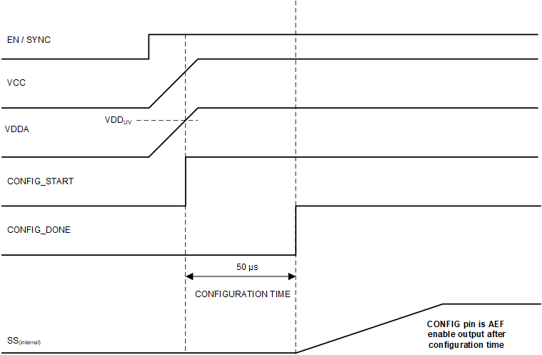
The LM5149 can be configured as a primary controller (interleaved mode) or as a secondary controller for paralleling the outputs for high-current applications with a resistor RCNFG. This resistor also configures if spread spectrum is enabled or disabled. See Table 8-2. After the VCC voltage is above 3.3 V (typical), the CNFG pin is monitored and latched. The configuration cannot be changed on the fly – the LM5149 must be powered down, and VCC must drop below 3.3 V. Figure 8-7 shows the configuration timing diagram.
When the LM5149 is configured as a primary controller with spread spectrum enabled (RCNFG of 41.2 kΩ or 71.5 kΩ), the LM5149 cannot be synchronized to an external clock.
| RCNFG | PRIMARY or SECONDARY | SPREAD SPECTRUM | DUAL PHASE |
|---|---|---|---|
| 29.9 kΩ | Primary | OFF | Disabled |
| 41.2 kΩ | Primary | ON | Disabled |
| 54.9 kΩ | Primary | OFF | Enabled |
| 71.5 kΩ | Primary | ON | Enabled |
| 90.9 kΩ | Secondary | N/A | Enabled |
 Figure 8-7 Configuration Timing
After the configuration has been latched, the CNFG pin become an enable input for the active EMI filter, where a logic high (> 2 V) enables the active EMI filter and a logic low (< 0.8 V) disables AEF.