SNVSAP6C September 2017 – October 2021 LM5150-Q1
PRODUCTION DATA
- 1 Features
- 2 Applications
- 3 Description
- 4 Revision History
- 5 Device Comparison Table
- 6 Pin Configuration and Functions
- 7 Specifications
-
8 Detailed Description
- 8.1 Overview
- 8.2 Functional Block Diagram
- 8.3
Feature Description
- 8.3.1 Enable (EN Pin)
- 8.3.2 High Voltage VCC Regulator (PVCC, AVCC Pin)
- 8.3.3 Power-On Voltage Selection (VSET Pin)
- 8.3.4 Switching Frequency (RT Pin)
- 8.3.5 Clock Synchronization (SYNC Pin in SS Configuration)
- 8.3.6 Current Sense, Slope Compensation, and PWM (CS Pin)
- 8.3.7 Current Limit (CS Pin)
- 8.3.8 Feedback and Error Amplifier (COMP Pin)
- 8.3.9 Automatic Wake-Up and Standby
- 8.3.10 Boost Status Indicator (STATUS Pin)
- 8.3.11 Maximum Duty Cycle Limit, Minimum Input Supply Voltage
- 8.3.12 MOSFET Driver (LO Pin)
- 8.3.13 Thermal Shutdown
- 8.4 Device Functional Modes
-
9 Application and Implementation
- 9.1 Application Information
- 9.2
Typical Application
- 9.2.1 Design Requirements
- 9.2.2
Detailed Design Procedure
- 9.2.2.1 Custom Design With WEBENCH® Tools
- 9.2.2.2 RSET Resistor
- 9.2.2.3 RT Resistor
- 9.2.2.4 Inductor Selection (LM)
- 9.2.2.5 Current Sense (RS)
- 9.2.2.6 Slope Compensation Ramp (RSL)
- 9.2.2.7 Output Capacitor (COUT)
- 9.2.2.8 Loop Compensation Component Selection and Maximum ESR
- 9.2.2.9 PVCC Capacitor, AVCC Capacitor, and AVCC Resistor
- 9.2.2.10 VOUT Filter (CVOUT, RVOUT)
- 9.2.2.11 Input Capacitor
- 9.2.2.12 MOSFET Selection
- 9.2.2.13 Diode Selection
- 9.2.2.14 Efficiency Estimation
- 9.2.3 Application Curves
- 9.3 System Examples
- 10Power Supply Recommendations
- 11Layout
- 12Device and Documentation Support
- 13Mechanical, Packaging, and Orderable Information
Package Options
Refer to the PDF data sheet for device specific package drawings
Mechanical Data (Package|Pins)
- RUM|16
Thermal pad, mechanical data (Package|Pins)
- RUM|16
Orderable Information
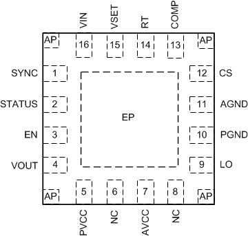
6 Pin Configuration and Functions
 Figure 6-1 16-Pin
WQFNRUM Package(Top View)
Figure 6-1 16-Pin
WQFNRUM Package(Top View)Table 6-1 Pin Functions
| PIN | I/O(3) | DESCRIPTION | |
|---|---|---|---|
| NO. | NAME | ||
| 1 | SYNC | I | External synchronization clock input pin. The internal oscillator is synchronized to an external clock by applying a pulse signal into the SYNC pin in the start-stop configuration. Connect directly to ground if not used or in emergency call configuration. Maximum duty cycle limit can be programmed by controlling the external synchronization clock frequency. |
| 2 | STATUS | O | Status indicator with an open-drain output stage. Internal pulldown switch holds the pin low when the device is not boosting. The pin can be left floating if not used. |
| 3 | EN | I | Enable pin. If EN is below 1 V, the device is in shutdown mode. The pin must be raised above 2 V to enable the device. Connect directly to VOUT pin for an automatic boost. |
| 4 | VOUT | I/P | Boost output voltage-sensing pin and input to VCC regulator. Connect to the output of the boost converter. |
| 5 | PVCC | O/P | Output of the VCC bias regulator. Decouple locally to PGND using a low-ESR or low-ESL ceramic capacitor located as close to the device as possible. |
| 6 | NC | — | No internal electrical connection. Leave the pin floating or connect directly to ground. |
| 7 | AVCC | I/P | Analog VCC supply input. Decouple locally to AGND using 0.1-µF low-ESR or low-ESL ceramic capacitor located as close to the device as possible. Connect to the PVCC pin through 10-Ω resistor. |
| 8 | NC | — | No internal electrical connection. Leave the pin floating or connect directly to ground. |
| 9 | LO | O | N-channel MOSFET gate drive output. Connect to the gate of the N-channel MOSFET through a short, low inductance path. |
| 10 | PGND | G | Power ground pin. Connect to the ground connection of the sense resistor through a wide and short path. |
| 11 | AGND | G | Analog ground pin. Connect to the analog ground plane through a wide and short path. |
| 12 | CS | I | Current sense input pin. Connect to the positive side of the current sense resistor through a short path. |
| 13 | COMP | O | Output of the internal transconductance error amplifier. The loop compensation components must be connected between this pin and AGND. |
| 14 | RT | I | Switching frequency setting pin. The switching frequency is programmed by a single resistor between RT and AGND. |
| 15 | VSET | I | Configuration selection and VOUT regulation target programming pin. During initial power on, a resistor between the VSET pin and AGND configures the VOUT regulation target and the configuration. |
| 16 | VIN | I | Boost input voltage sensing pin. Connect to the input supply of the boost converter. |
| — | EP | — | Exposed pad of the package. No internal electrical connection to silicon die. The EP is electrically connected to anchor pads. The EP must be connected to the large ground copper plain to reduce thermal resistance. |
| — | AP | — | Anchor pad of the package. No internal electrical connection to silicon die. The AP is electrically connected to the EP. The AP can be left floating or soldered to the ground copper. |
(3) G = Ground, I = Input, O = Output, P = Power