SNVSBI7B January 2020 – January 2021 LM5156-Q1 , LM51561-Q1
PRODUCTION DATA
- 1 Features
- 2 Applications
- 3 Description
- 4 Revision History
- 5 Description (continued)
- 6 Device Comparison Table
- 7 Pin Configuration and Functions
- 8 Specifications
-
9 Detailed Description
- 9.1 Overview
- 9.2 Functional Block Diagram
- 9.3
Feature Description
- 9.3.1 Line Undervoltage Lockout (UVLO/SYNC/EN Pin)
- 9.3.2 High Voltage VCC Regulator (BIAS, VCC Pin)
- 9.3.3 Soft Start (SS Pin)
- 9.3.4 Switching Frequency (RT Pin)
- 9.3.5 Dual Random Spread Spectrum (DRSS)
- 9.3.6 Clock Synchronization (UVLO/SYNC/EN Pin)
- 9.3.7 Current Sense and Slope Compensation (CS Pin)
- 9.3.8 Current Limit and Minimum On-time (CS Pin)
- 9.3.9 Feedback and Error Amplifier (FB, COMP Pin)
- 9.3.10 Power-Good Indicator (PGOOD pin)
- 9.3.11 Hiccup Mode Overload Protection (LM51561-Q1 Only)
- 9.3.12 Maximum Duty Cycle Limit and Minimum Input Supply Voltage
- 9.3.13 MOSFET Driver (GATE Pin)
- 9.3.14 Overvoltage Protection (OVP)
- 9.3.15 Thermal Shutdown (TSD)
- 9.4 Device Functional Modes
- 10Application and Implementation
- 11Power Supply Recommendations
- 12Layout
- 13Device and Documentation Support
- 14Mechanical, Packaging, and Orderable Information
Package Options
Mechanical Data (Package|Pins)
- DSS|12
Thermal pad, mechanical data (Package|Pins)
- DSS|12
Orderable Information
7 Pin Configuration and Functions
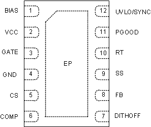
 Figure 7-1 12-Pin WSON With Wettable
FlanksDSS Package(Transparent Top View)
Figure 7-1 12-Pin WSON With Wettable
FlanksDSS Package(Transparent Top View)Table 7-1 Pin Functions
| PIN | TYPE(1) | DESCRIPTION | |
|---|---|---|---|
| NO. | NAME | ||
| 1 | BIAS | P | Supply voltage input to the VCC regulator. Connect a bypass capacitor from this pin to GND. |
| 2 | VCC | P | Output of the internal VCC regulator and supply voltage input of the MOSFET driver. Connect a ceramic bypass capacitor from this pin to GND. |
| 3 | GATE | O | N-channel MOSFET gate drive output. Connect directly to the gate of the N-channel MOSFET through a short, low inductance path. |
| 4 | GND | G | Ground pin. Connect directly to the ground connection of the sense resistor through a low inductance wide and short path. |
| 5 | CS | I | Current sense input pin. Connect to the positive side of the current sense resistor through a short path. |
| 6 | COMP | O | Output of the internal transconductance error amplifier. Connect the loop compensation components between this pin and GND. |
| 7 | DITHOFF | I | Spread spectrum selection pin. Internal spread spectrum (Clock dithering) is disabled when the pin is connected to the VCC pin. Connecting the pin to GND enables the internal spread spectrum. |
| 8 | FB | I | Inverting input of the error amplifier. Connect a voltage divider from the output to this pin to set output voltage in boost/SEPIC topologies. Connect the low-side feedback resistor to GND. |
| 9 | SS | I | Soft-start time programming pin. An external capacitor and an internal current source set the ramp rate of the internal error amplifier reference during soft start. Connect the ground connection of the capacitor to GND. |
| 10 | RT | I | Switching frequency setting pin. The switching frequency is programmed by a single resistor between RT and GND. |
| 11 | PGOOD | O | Power-good indicator. An open-drain output which goes low if FB is below the under voltage threshold. Connect a pullup resistor to the system voltage rail. |
| 12 | UVLO/SYNC/EN | I | Undervoltage lockout programming pin. The converter start-up and shutdown levels can be programmed by connecting this pin to the supply voltage through a resistor divider. The internal clock can be synchronized to an external clock by applying a negative pulse signal into the UVLO/SYNC/EN pin. This pin must not be left floating. Connect to BIAS pin if not used. Connect the low-side UVLO resistor to GND. |
| — | EP | — | Exposed pad of the package. The exposed pad must be connected to GND and the large ground copper plane to decrease thermal resistance. |
(1) G = Ground, I = Input, O = Output, P = Power