SNVSA03E October   2014  – October 2018 LM5160 , LM5160A

PRODUCTION DATA.  

  1. Features
  2. Applications
  3. Description
    1.     Device Images
      1.      Typical Synchronous Buck Application Circuit
      2.      Typical Fly-Buck Application Circuit
  4. Revision History
  5. Pin Configuration and Functions
    1.     Pin Functions
  6. Specifications
    1. 6.1 Absolute Maximum Ratings
    2. 6.2 ESD Ratings
    3. 6.3 Recommended Operating Conditions
    4. 6.4 Thermal Information
    5. 6.5 Electrical Characteristics
    6. 6.6 Switching Characteristics
    7. 6.7 Typical Characteristics
  7. Detailed Description
    1. 7.1 Overview
    2. 7.2 Functional Block Diagram
    3. 7.3 Feature Description
      1. 7.3.1  Control Circuit
      2. 7.3.2  VCC Regulator
      3. 7.3.3  Regulation Comparator
      4. 7.3.4  Soft Start
      5. 7.3.5  Error Amplifier
      6. 7.3.6  On-Time Generator
      7. 7.3.7  Current Limit
      8. 7.3.8  N-Channel Buck Switch and Driver
      9. 7.3.9  Synchronous Rectifier
      10. 7.3.10 Enable / Undervoltage Lockout (EN/UVLO)
      11. 7.3.11 Thermal Protection
    4. 7.4 Device Functional Modes
      1. 7.4.1 Forced Pulse Width Modulation (FPWM) Mode
      2. 7.4.2 Undervoltage Detector
  8. Application and Implementation
    1. 8.1 Application Information
      1. 8.1.1 Ripple Configuration
    2. 8.2 Typical Applications
      1. 8.2.1 LM5160 Synchronous Buck (10-V to 60-V Input, 5-V Output, 1.5-A Load)
        1. 8.2.1.1 Design Requirements
        2. 8.2.1.2 Detailed Design Procedure
          1. 8.2.1.2.1  Custom Design With WEBENCH® Tools
          2. 8.2.1.2.2  Feedback Resistor Divider - RFB1, RFB2
          3. 8.2.1.2.3  Switching Frequency - RON
          4. 8.2.1.2.4  Inductor - L
          5. 8.2.1.2.5  Output Capacitor - COUT
          6. 8.2.1.2.6  Series Ripple Resistor - RESR
          7. 8.2.1.2.7  VCC and Bootstrap Capacitors - CVCC, CBST
          8. 8.2.1.2.8  Input Capacitor - CIN
          9. 8.2.1.2.9  Soft-Start Capacitor - CSS
          10. 8.2.1.2.10 EN/UVLO Resistors - RUV1, RUV2
        3. 8.2.1.3 Application Curves
      2. 8.2.2 LM5160 Isolated Fly-Buck (18-V to 32-V Input, 12-V, 4.5-W Isolated Output)
        1. 8.2.2.1 LM5160 Fly-Buck Design Requirements
        2. 8.2.2.2 Detailed Design Procedure
          1. 8.2.2.2.1 Selection of VOUT1 and Turns Ratio
          2. 8.2.2.2.2 Secondary Rectifier Diode
          3. 8.2.2.2.3 External Ripple Circuit
          4. 8.2.2.2.4 Output Capacitor - COUT2
        3. 8.2.2.3 Application Curves
      3. 8.2.3 LM5160A Isolated Fly-Buck (18-V to 32-V Input, 12-V, 4.5-W Isolated Output)
    3. 8.3 Do's and Don'ts
  9. Power Supply Recommendations
  10. 10Layout
    1. 10.1 Layout Guidelines
    2. 10.2 Layout Example
  11. 11Device and Documentation Support
    1. 11.1 Device Support
      1. 11.1.1 Third-Party Products Disclaimer
      2. 11.1.2 Development Support
        1. 11.1.2.1 Custom Design With WEBENCH® Tools
    2. 11.2 Documentation Support
      1. 11.2.1 Related Documentation
    3. 11.3 Related Links
    4. 11.4 Receiving Notification of Documentation Updates
    5. 11.5 Community Resources
    6. 11.6 Trademarks
    7. 11.7 Electrostatic Discharge Caution
    8. 11.8 Glossary
  12. 12Mechanical, Packaging, and Orderable Information

Package Options

Mechanical Data (Package|Pins)
Thermal pad, mechanical data (Package|Pins)
Orderable Information

Typical Characteristics

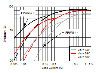
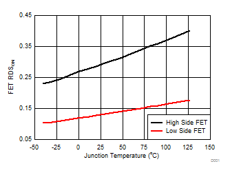
TA = 25°C and applicable to both LM5160 and LM5160A, unless otherwise noted. Please refer to Typical Applications for circuit designs.
LM5160 LM5160A Eff_10Vo_Updated_SNVSA03.gif
VOUT = 10 V RON = 200 kΩ
L = 47 µH
Figure 1. Efficiency at 500 kHz
LM5160 LM5160A CCM_DCM_Eff_SNVSA03.gif
VOUT = 5 V RON = 169 kΩ
L = 47 µH
Figure 3. Efficiency CCM vs DCM at 300 kHz
LM5160 LM5160A Vcc_Vin_SNVSA03.gif
Figure 5. VCC vs VIN
LM5160 LM5160A ILim_OffTimer_SNVSA03.gif
Figure 7. TOFF (ILIM) vs VFB
LM5160 LM5160A Fsw_Vin_SNVSA03.gif
VOUT = 5 V
Figure 9. Switching Frequency vs VIN
LM5160 LM5160A Gate Drive UVLO_Revised_SNVSA03.gif
VIN = 24 V
Figure 11. Gate Drive UVLO vs Temperature
LM5160 LM5160A Operating Current_SNVSA03.gif
VIN = 24 V
Figure 13. Input Operating Current vs Temperature
LM5160 LM5160A Vcc UVLO Threshold_SNVSA03.gif
VIN = 24 V
Figure 15. VCC UVLO vs Temperature
LM5160 LM5160A FPWM_Revised_SNVSA03.gif
VIN = 24 V
Figure 17. FPWM Threshold vs Temperature
LM5160 LM5160A Eff_250kHz_SNVSA03.gif
VOUT = 5 V RON = 215 kΩ
L = 100 µH
Figure 2. Efficiency at 250 kHz
LM5160 LM5160A Eff vs Vin Updated_SNVSA03.gif
VOUT = 5 V RON = 169 kΩ
L = 47 µH
Figure 4. Efficiency vs Input Voltage at 300 kHz
LM5160 LM5160A Vcc_Icc_SNVSA03.gif
VIN = 24 V
Figure 6. VCC vs ICC
LM5160 LM5160A On-Time_Vin_SNVSA03.gif
VOUT = 5 V
Figure 8. TON vs VIN
LM5160 LM5160A Operating Current vs. Vin _Revised_SNVSA03.gif
VFB = 3 V
Figure 10. IIN vs VIN (Operating, Non-Switching)
LM5160 LM5160A Vref_vs_Temp_LM5160_SNVSA03.gif
VIN = 24 V
Figure 12. Reference Voltage vs Temperature
LM5160 LM5160A Shutdown_Current_SNVSA03.gif
VIN = 24 V
Figure 14. Input Shutdown Current vs Temperature
LM5160 LM5160A Current Limit_SNVSA03.gif
VIN = 24 V
Figure 16. Current Limit vs Temperature
LM5160 LM5160A FET_Rdson_SNVSA03.gif
ISW = 200 mA VIN = 24 V
Figure 18. Switch Resistance vs Temperature