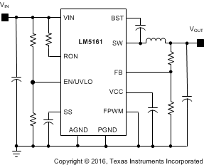
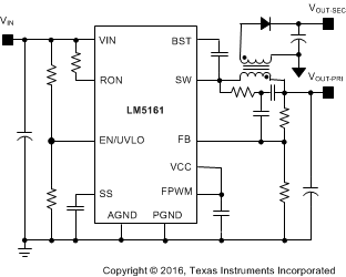
The LM5161 is a 100-V, 1-A synchronous step-down converter with integrated high-side and low-side MOSFETs. The constant-ON-time control scheme requires no loop compensation and supports high step-down ratios with fast transient response. An internal feedback amplifier maintains ±1% output voltage regulation over the entire operating temperature range. The ON-time varies inversely with input voltage resulting in nearly constant switching frequency. Peak and valley current limit circuits protect against overload conditions. The under-voltage lockout (EN/UVLO) circuit provides independently adjustable input undervoltage threshold and hysteresis. The FPWM input pin in LM5161 selects either the forced continuous conduction mode (CCM) under all load levels or the discontinuous conduction mode (DCM) under light or no load conditions. When operating in forced CCM, the LM5161 supports the multiple output and isolated Fly-Buck applications. When programmed for the DCM operation, the LM5161 provides a tightly regulated buck output without any additional external feedback ripple injection circuit.
PART NUMBER | PACKAGE | BODY SIZE (NOM) |
---|---|---|
LM5161 | HTSSOP (14) | 5.00 mm × 4.40 mm |
PIN | I/O | DESCRIPTION | |
---|---|---|---|
NAME | HTSSOP | ||
AGND | 1 | - | Analog ground. Ground connection of internal control circuits. |
PGND | 2 | - | Power ground. Ground connection of the internal synchronous rectifier FET. |
VIN | 3 | I | Input supply connection. Operating input range is 4.5-V to 100-V. |
EN/UVLO | 4 | I | Precision enable. Input pin of undervoltage lockout (UVLO) comparator. |
RON | 5 | I | On-time programming pin. A resistor between this pin and VIN sets the switch ON-time as a function of input voltage. |
SS | 6 | I | Soft start. Connect a capacitor from SS to AGND to control output rise time and limit overshoot. |
FPWM | 8 | I | Forced PWM logic input pin. Connect to AGND for discontinuous conduction mode (DCM) with light loads. Connect to VCC for continuous conduction mode (CCM) at all loads and Fly-Buck configuration. |
FB | 9 | I | Feedback input of voltage regulation comparator. |
VCC | 10 | O | Internal high voltage start-up regulator bypass capacitor pin. |
BST | 11 | I | Bootstrap capacitor pin. Connect a capacitor between BST and SW to bias gate driver of high-side buck FET. |
SW | 12,13 | O | Switch node. Source connection of high side buck FET and drain connection of low-side synchronous rectifier FET. |
NC | 7,14 | No connection | |
EP | - | Exposed pad. Connect to AGND and printed-circuit board ground plane to improve power dissipation. |
MIN | MAX | UNIT | ||
---|---|---|---|---|
Input voltage | VIN to AGND | –0.3 | 100 | V |
EN/UVLO to AGND | –0.3 | 100 | ||
RON to AGND | –0.3 | 100 | ||
BST to AGND | –0.3 | 114 | ||
VCC to AGND | –0.3 | 14 | ||
FPWM to AGND | –0.3 | 14 | ||
SS to AGND | –0.3 | 7 | ||
FB to AGND | –0.3 | 7 | ||
Output voltage | BST to SW | –0.3 | 14 | V |
BST to VCC | 100 | |||
SW to AGND | –1.5 | 100 | ||
SW to AGND (20-ns transient) | –3 | |||
Maximum junction temperature(3) | –40 | 150 | °C | |
Storage temperature Tstg | –65 | 150 | °C |
VALUE | UNIT | |||
---|---|---|---|---|
V(ESD) | Electrostatic discharge | Human-body model (HBM), per ANSI/ESDA/JEDEC JS-001(1) | ±2000 | V |
Charged-device model (CDM), per JEDEC specification JESD22-C101(2) | ±750 |
MIN | NOM | MAX | UNIT | ||
---|---|---|---|---|---|
VIN input voltage | 4.5 | 100 | V | ||
IO output current | 1 | A | |||
External VCC bias voltage | 9 | 13 | V | ||
Operating junction temperature(2) | –40 | 125 | °C |
THERMAL METRIC | LM5161 | UNIT | |
---|---|---|---|
PWP (HTSSOP) | |||
14 PINS | |||
RθJA | Junction-to-ambient thermal resistance(1) | 39.3 | °C/W |
RθJCbot | Junction-to-case (bottom) thermal resistance(1) | 2.0 | °C/W |
ψJB | Junction-to-board thermal characteristic parameter | 19.3 | °C/W |
RθJB | Junction-to-board thermal resistance | 19.6 | °C/W |
RθJCtop | Junction-to-case (top) thermal resistance | 22.8 | °C/W |
ψJT | Junction-to-top thermal characteristic parameter | 0.5 | °C/W |
PARAMETER | TEST CONDITIONS | MIN | TYP | MAX | UNIT | |
---|---|---|---|---|---|---|
SUPPLY CURRENT | ||||||
ISD | Input shutdown current | VIN = 48 V, EN/UVLO = 0 V | 50 | 90 | µA | |
IOP | Input operating current | VIN = 48 V, FB = 3 V, Non-switching | 2.3 | 2.8 | mA | |
VCC SUPPLY | ||||||
VCC | Bias regulator output | VIN = 48 V, ICC = 20 mA | 6.3 | 7.3 | 8.5 | V |
VCC | Bias regulator current limit | VIN = 48 V | 30 | mA | ||
VCC(UV) | VCC undervoltage threshold | VCC rising | 3.98 | 4.1 | V | |
VCC(HYS) | VCC undervoltage hysteresis | VCC falling | 185 | mV | ||
VCC(LDO) | VIN - VCC dropout voltage | VIN = 4.5 V, ICC = 20 mA | 200 | 340 | mV | |
HIGH-SIDE FET | ||||||
RDS(ON) | High-side on resistance | V(BST - SW) = 7 V, ISW = 0.5A | 0.58 | Ω | ||
BST(UV) | Bootstrap gate drive UV | V(BST - SW) rising | 2.93 | 3.6 | V | |
BST(HYS) | Gate drive UV hysteresis | V(BST - SW) falling | 200 | mV | ||
LOW-SIDE FET | ||||||
RDS(ON) | Low-side on resistance | ISW = 0.5 A | 0.24 | Ω | ||
HIGH-SIDE CURRENT LIMIT | ||||||
ILIM (HS) | High-side current limit threshold | 1.3 | 1.61 | 1.9 | A | |
TRES | Current limit response time | ILIM (HS)threshold detect to FET turn-off | 100 | ns | ||
TOFF | Current limit forced off-time | FB = 0 V, VIN = 72 V | 13 | 16.5 | 21 | µs |
TOFF1 | Current limit forced off-time | FB = 0.1 V, VIN = 72 V | 10 | 13 | 17 | µs |
TOFF2 | Current limit forced off-time | FB = 1 V, VIN = 72 V | 2 | 2.7 | 4.1 | µs |
LOW-SIDE CURRENT LIMIT | ||||||
ISOURCE(LS) | Sourcing current limit | 1.3 | 1.6 | 1.9 | A | |
ISINK(LS) | Sinking current limit | 3 | ||||
DIODE EMULATION | ||||||
VFPWM(LOW) | FPWM input logic low | VIN = 48 V | 1 | V | ||
VFPWM(HIGH) | FPWM input logic high | VIN = 48 V | 3 | |||
IZX | Zero cross detect current | FPWM = 0 (Diode emulation) | 22.5 | mA | ||
REGULATION COMPARATOR | ||||||
VREF | FB regulation level | VIN = 48 V | 1.975 | 2 | 2.015 | V |
I(BIAS) | FB input bias current | VIN = 48 V | 100 | nA | ||
ERROR CORRECTION AMPLIFIER AND SOFT START | ||||||
GM | Error amp transconductance | FB = VREF (±) 10 mV | 100 | µA/V | ||
IEA(SOURCE) | Error amp source current | FB = 1 V, SS = 1 V | 7.5 | 10 | 12.5 | µA |
IEA(SINK) | Error amp sink current | FB = 5 V, SS = 2.25 V | 7.5 | 10 | 12.5 | |
V(SS-FB) | VSS - VFB clamp voltage | FB = 1.75 V, CSS= 1 nF | 135 | mV | ||
ISS | Soft-start charging current | SS = 0.5 V | 7.5 | 10 | 12.5 | µA |
ENABLE/UVLO | ||||||
VUVLO (TH) | UVLO threshold | EN/UVLO rising | 1.195 | 1.24 | 1.272 | V |
IUVLO(HYS) | UVLO hysteresis current | EN/UVLO = 1.4 V | 15 | 20 | 25 | µA |
VSD(TH) | Shutdown mode threshold | EN/UVLO falling | 0.29 | 0.35 | V | |
VSD(HYS) | Shutdown threshold hysteresis | EN/UVLO rising | 50 | mV | ||
THERMAL SHUTDOWN | ||||||
TSD | Thermal shutdown threshold | 175 | °C | |||
TSD(HYS) | Thermal shutdown hysteresis | 20 | °C |
PARAMETER | TEST CONDITIONS | MIN | TYP | MAX | UNIT | |
---|---|---|---|---|---|---|
MINIMUM OFF-TIME | ||||||
TOFF-MIN | Minimum off-time, FB = 0 V | 170 | ns | |||
TOFF-MIN | Minimum off-time, FB = 0 V, VIN = 4.5 V | 200 | ns | |||
ON-TIME GENERATOR | ||||||
TON Test 1 | VIN = 24 V, RON = 100 kΩ | 420 | 540 | 665 | ns | |
TON Test 2 | VIN = 48 V, RON = 100 kΩ | 270 | ns | |||
TON Test 3 | VIN = 8 V, RON = 100 kΩ | 1150 | 1325 | 1500 | ns | |
TON Test 4 | VIN = 72V, RON = 150 kΩ | 285 | ns |
VOUT = 3.3 V | RON = 110 kΩ | |
FPWM = 0 |
VOUT = 12 V | RON = 402 kΩ | |
FPWM = 0 | L = 100 µH |
VOUT = 12 V | RON = 300 kΩ | |
FPWM = 1 | L = 100 µH |
VIN = 48 V | ||
VIN = 48 V | ||
VIN = 48 V | ||
VIN = 48 V | ||
VIN = 48 V | ||
VOUT = 5 V | RON = 169 kΩ | |
L=47 µH |
VOUT = 12 V | RON = 402 kΩ | |
FPWM = 1 | L = 100 µH |
IOUT = 1 A | FPWM = 0 | |
VOUT = 12 V | ||
VFB = 3 V | ||
VIN = 48 V | ||
VIN = 48 V | ||
VIN = 48 V | ||
VIN = 48 V | ||
ISW = 500 mA | VIN = 48 V | |
The LM5161 step-down switching regulator features all the functions needed to implement a low-cost, efficient buck converter capable of supplying 1-A to the load. This high voltage regulator contains 100-V N-channel buck and synchronous rectifier switches and is available in the 14-pin HTSSOP package. The regulator operation is based on constant ON-time control where the ON-time is inversely proportional to input voltage VIN. This feature maintains a relatively constant operating frequency with load and input voltage variations. A constant on-time switching regulator requires no loop compensation resulting in fast load transient response. Peak current limit detection circuit is implemented with a forced OFF-time during current limiting which is inversely proportional to voltage at the feedback pin, VFB and directly proportional to VIN. Varying the current limit OFF-time with VFB and VIN ensures short circuit protection with minimal current limit foldback. The LM5161 can be applied in numerous end equipment systems requiring efficient step-down regulation from higher input voltages. This regulator is well suited for 24 V industrial systems as well as for 48 V telecom and PoE voltage ranges. The LM5161 integrates an under-voltage lockout (EN/UVLO) circuit to prevent faulty operation of the device at low input voltages and features intelligent current limit and thermal shutdown to protect the device during overload or short circuit.
The LM5161 step-down switching regulator employs a control principle based on a comparator and a one-shot ON-timer, with the output voltage feedback (FB) compared to the voltage at the Soft-Start (SS) pin (VSS). If the FB voltage is below VSS, the internal buck switch is turned on for a time period determined by the input voltage and one-shot programming resistor (RON). Following the ON-time, the buck switch must remain off for the minimum OFF-time forced by the minimum OFF-time one-shot. The buck switch remains off until the FB voltage falls below VSS again, when it turns on for another ON-time one-shot period.
During a rapid start-up or when the load current increases suddenly, the regulator operates with minimum off-time per cycle. When regulating the output in steady state operation, the off-time automatically adjusts to produce the SW pin duty cycle required for output voltage regulation.
When in regulation, the LM5161 operates in continuous conduction mode at heavy load currents. If the FPWM pin is connected to ground or left floating, the regulator operates in discontinuous conduction mode at light load with the synchronous rectifier FET emulating a diode. With sufficient load, the LM5161 operates in continuous conduction mode with the inductor current never reaching zero during the OFF-time of the high-side FET. In this mode the operating frequency remains relatively constant with load and line variations. The minimum load current for continuous conduction mode is one-half the inductor’s ripple current amplitude. The operating frequency (in Hz) is programmed by the RON pin resistor and can be calculated from Equation 1 with RON expressed in ohms.
In discontinuous conduction mode, current through the inductor ramps up from zero to a peak value during the ON-time, then ramps back to zero before the end of the OFF-time. The next ON-time period starts when the voltage at FB falls below VSS. When the inductor current is zero during the high side FET off-time, the load current is supplied by the output capacitor. In this mode, the operating switching frequency is lower than the continuous conduction mode switching frequency and the frequency varies with load. The discontinuous conduction mode maintains higher conversion efficiency at light loads because the switching losses decrease with the decrease in load and frequency.
The output voltage is set by two external resistors ( RFB1, RFB2). The regulated output voltage is calculated from Equation 2, where VREF = 2 V (typ) is the feedback reference voltage.
The LM5161 contains an internal high voltage linear regulator with a nominal output voltage of 7.3 V (typical). The VCC regulator is internally current limited to 30 mA (minimum). This regulator supplies power to internal circuit blocks including the synchronous FET gate driver and the logic circuits. When the voltage on the VCC pin reaches the undervoltage lockout (VCC(UV)) threshold of 3.98 V (typical), the IC is enabled. An external capacitor at the VCC pin stabilizes the regulator and supplies transient VCC current to the gate drivers. An internal diode connected from VCC to the BST pin replenishes the charge in the high-side gate drive bootstrap capacitor when the SW pin is low.
In high input voltage applications, the power dissipated in the regulator is significant and can limit the efficiency and maximum achievable output power. The LM5161 allows the internal VCC regulator power loss to be reduced by supplying the VCC voltage via a diode from an external voltage source regulated between 9 V and 13 V. The external VCC bias can be supplied from the LM5161 converter output rail if the regulation voltage is within this range. When the VCC pin of the LM5161 is raised above the regulation voltage (7.3 V typical), the internal regulator is disabled and the power dissipation in the IC is reduced.
The feedback voltage at the FB pin is compared to the SS pin voltage VSS. In normal operation when the output voltage is in regulation, an ON-time period is initiated when the voltage at FB pin falls below VSS. The high-side buck switch stays on for the ON-time one-shot period causing the FB voltage to rise. After the on-time period expires, the high-side switch will remain off until the FB voltage falls below VSS. During start-up, the FB voltage is below VSS at the end of each on-time period and the high-side switch turns on again after the minimum forced off-time of 170 ns (typical). When the output is shorted to ground (FB = 0 V), the high side peak current limit is triggered, the high-side FET is turned off, and remains off for a period determined by the current limit OFF-time one-shot. See the Current Limit section for additional information.
The soft-start feature of the LM5161 allows the converter to gradually reach a steady-state operating point, thereby reducing start-up stresses and current surges. When the EN/UVLO pin is above the EN/UVLO standby threshold VUVLO(TH) = 1.24 V (typ) and VCC exceeds the VCC undervoltage VCC(UV) = 3.98 V (typ) threshold, an internal 10-µA current source charges the external capacitor at the SS pin (CSS) from 0 V to 2 V. The voltage at the SS pin is connected to the noninverting input of the internal FB comparator. The soft-start interval ends when the SS capacitor is charged to the 2 V reference level. The ramping voltage at the SS pin produces a controlled, monotonic output voltage start-up. A minimum 1-nF soft-start capacitor must be used in all applications.
The LM5161 provides a trans-conductance (GM) error amplifier that minimizes the difference between the reference voltage (VREF) and the average feedback (FB) voltage. This amplifier reduces the load and line regulation errors that are common in constant-on-time regulators. The soft-start capacitor (CSS) provides compensation for this error correction loop. The soft-start capacitor should be greater than 1 nF to ensure stability.
The ON-time of the LM5161 high-side FET is determined by the RON resistor and is inversely proportional to the input voltage (VIN). The inverse relationship with VIN results in a nearly constant frequency as VIN is varied. The ON-time can be calculated from Equation 3 with RON expressed in ohms.
To set a specific continuous conduction mode switching frequency (FSW expressed in Hz), the RON resistor is determined from Equation 4:
RON must be selected for a minimum on-time (at maximum VIN) greater than 150 ns for proper operation. This minimum ON-time requirement limits the maximum switching frequency of applications with relatively high VIN and low VOUT.
The LM5161 provides an intelligent current limit OFF-timer that adjusts the OFF-time to reduce foldback of the current limit. If the peak value of the current in the buck switch exceeds 1.6 A (typical) the present ON-time period is immediately terminated, and a non-resettable OFF-timer is initiated. The length of the OFF-time is controlled by the FB voltage and the input voltage VIN. As an example, when VFB = 0.1-V and VIN = 72-V, the OFF-time is set to 13 μs (typical). This condition would occur if the output is shorted or during the initial phase of start-up. In cases of output overload where the FB voltage is greater than zero volts (a soft short), the current limit OFF-time is reduced. Reducing the OFF-time during less severe overloads reduces the current limit foldback, overload recovery time, and start-up time. The current limit off-time, TOFF(CL) is calculated from Equation 5:
The LM5161 integrates an N-channel buck switch and associated floating high-side gate driver. The gate driver circuit works in conjunction with an external bootstrap capacitor and an internal high voltage bootstrap diode. A 10-nF or larger ceramic capacitor connected between the BST pin and the SW pin provides the voltage to the high-side driver during the buck switch ON-time. During the OFF-time, the SW node is pulled down to approximately 0 V and the bootstrap capacitor charges from VCC through the internal bootstrap diode. The minimum OFF-time of 170 ns (typical) provides a minimum time each cycle to recharge the bootstrap capacitor.
The LM5161 provides an internal low-side synchronous rectifier N-channel FET. This low-side FET provides a low resistance path for the inductor current when the high-side FET is turned off.
With the FPWM pin connected to ground or left floating, the LM5161 synchronous rectifier operates in diode emulation mode. Diode emulation enables the pulse-skipping during light load conditions. This leads to a reduction in the average switching frequency at light loads. Switching losses and FET gate driver losses, both of which are proportional to switching frequency, are significantly reduced and efficiency is improved. This pulse-skipping mode also reduces the circulating inductor currents and losses associated with a continuous conduction mode (CCM). When the FPWM pin is grounded or left floating, an internal ripple injection circuit is enabled. With the internal ripple injection enabled, the typical external feedback ripple injection circuit is no longer required. This feature reduces the component count in the buck applications. For more details see Forced Pulse Width Modulation (FPWM) Mode.
When the FPWM pin is pulled high, diode emulation is disabled. The inductor current can flow in either direction through the low-side FET resulting in CCM operation with nearly constant switching frequency. A negative sink current limit circuit limits the current that can flow into the SW pin and through the low-side FET to ground. In a buck regulator application, large negative current will only flow from VOUT to the SW pin if VOUT is lifted above the output regulation set-point.
The LM5161 contains a dual level undervoltage lockout (EN/UVLO) circuit. When the EN/UVLO pin voltage is below 0.35 V (typical), the regulator is in a low current shutdown mode. When the EN/UVLO pin voltage is greater than 0.35 V (typical) but less than 1.24 V (typical), the regulator is in standby mode. In standby mode, the VCC bias regulator is active but converter switching remains disabled. When the voltage at the VCC pin exceeds the VCC rising threshold VCC(UV) = 3.98 V (typ) and the EN/UVLO pin voltage is greater than 1.24 V, normal switching operation begins. An external resistor voltage divider from VIN to GND can be used to set the minimum operating voltage of the regulator.
EN/UVLO hysteresis is accomplished with an internal 20-μA (typical) current source (IUVLO(HYS)) that is switched on or off into the impedance of the EN/UVLO pin resistor divider. When the EN/UVLO threshold is exceeded, the current source is activated to effectively raise the voltage at the EN/UVLO pin. The hysteresis is equal to the value of this current times the upper resistance of the resistor divider, (RUV2) (See Functional Block Diagram.)
The LM5161 must be operated such that the junction temperature does not exceed 150°C during normal operation. An internal thermal shutdown circuit is provided to protect the LM5161 in the event of a higher than normal junction temperature. When activated, typically at 175°C, the controller is forced into a low-power reset state, disabling the high side buck switch and the VCC regulator. This feature prevents catastrophic failures due to device overheating. When the junction temperature falls below 155 °C (typical hysteresis = 20°C), the VCC regulator is enabled, and operation resumes.
The Synchronous Rectifier section gives a brief introduction to the LM5161 diode emulation feature. The FPWM pin allows the power supply designer to select either CCM or DCM mode of operation at light loads. When the FPWM pin is connected to ground or left floating (FPWM = 0), a pulse-skipping mode and the zero-cross current detector circuit is enabled. The zero-cross detector turns off the low-side FET when the inductor current falls close to zero (IZX, see Electrical Characteristics ). This feature allows the LM5161 regulator to operate in DCM mode at light loads. In the DCM state, the switching frequency decreases with lighter loads.
When the FPWM pin is left open or shorted to ground, the user can take the advantage of the internal ripple injection circuit, enabled in this mode, for a typical Buck application circuit. This feature is applicable over the entire load and input voltage ranges. It eliminates the need for an external feedback ripple injection circuit.
For wide VIN applications where VIN > 72 V, an external VCC supply is commonly used to minimize the power dissipation in the IC. In such applications at TJ >125°C, it is recommended to add a BST resistor (> 3Ω) in series with the BST capacitor, in order to protect the internal VCC-BST diode during a full load transient operation. The addition of the external resistor will reduce the fast (dv/dt) of the switch node that can impact the normal IC operation.
If the FPWM pin is pulled high, the LM5161 will operate in CCM mode regardless of the load conditions. The CCM operation reduces efficiency at light load but improves the output transient response to step load changes and provides nearly constant switching frequency. Moreover, the Fly-Buck topology always requires the continuous conduction mode during its operation.
The internal ripple injection circuit is disabled in the CCM mode. An external ripple injection circuit or an additional ESR resistor in series with the output capacitor is required to generate the optimal ripple at the FB node. Also, there is no need to add any BST resistor in series with the BST capacitor in either forced CCM Buck or Fly-Buck application.
FPWM PIN CONNECTION | LOGIC STAGE | DESCRIPTION |
---|---|---|
GND or Floating (High Z) | 0 | The FPWM pin is grounded or left floating. DCM enabled at light loads. Internal Ripple circuit is enabled. No external ripple circuit/ addition required. |
VCC | 1 | The FPWM pin is connected to VCC. The LM5161 then operates in CCM mode at light loads. Internal ripple injection disabled. External ripple injection needed. |
Table 2 summarizes the dual threshold levels of the under-voltage lockout (EN/UVLO) circuit explained in Enable / Undervoltage Lockout (EN/UVLO) .
EN/UVLO PIN VOLTAGE | VCC REGULATOR | MODE | DESCRIPTION |
---|---|---|---|
< 0.35 V | Off | Shutdown | VCC regulator disabled. High and low side FETs disabled. |
0.35 V to 1.24 V | On | Standby | VCC regulator enabled. High and low side FETs disabled. |
> 1.24 V | VCC < VCC(UV) | Standby | VCC regulator enabled. High and low side FETs disabled. |
VCC > VCC(UV) | Operating | VCC regulator enabled. Switching enabled. |
If an EN/UVLO setpoint is not required, the EN/UVLO pin can be driven by a logic signal as an enable input or connected directly to the VIN pin. If the EN/UVLO is directly connected to the VIN pin, the regulator will begin switching when the VCC UVLO is satisfied.
NOTE
Information in the following applications sections is not part of the TI component specification, and TI does not warrant its accuracy or completeness. TI’s customers are responsible for determining suitability of components for their purposes. Customers should validate and test their design implementation to confirm system functionality.
The LM5161 is a synchronous-buck regulator converter designed to operate over a wide input voltage and output current range. Spreadsheet based Quick-Start Calculator tools, available on the www.ti.com product website, can be used to design a single output synchronous buck converter or an isolated dual output Fly-Buck converter using the LM5161. See application note Designing an Isolated Buck (Fly-Buck) Converter for a detailed design guide for the Fly-Buck converter. Alternatively, the online WEBENCH® Tool can be used to create a complete buck or Fly-Buck designs and generate the bill of materials, estimated efficiency, solution size, and cost of the complete solution.Typical Applications describes a few application circuits using the LM5161 with detailed, step-by-step design procedures.
A typical application example is a synchronous buck converter operating from a wide input voltage range of 15 V to 95 V and providing a stable 12 V output voltage with maximum output current capability of 1 A. The complete schematic for a typical buck application circuit with LM5161 in diode emulation is shown in Figure 25 . In the application schematic below, the components are labeled by their respective component numbers instead of the descriptive name used in the previous sections. For example, R1 represents RON and so on.
A typical synchronous-buck application introduced in LM5161 Synchronous Buck (15-V to 95-V Input, 12-V Output, 1-A Load) , Table 3 summarizes the operating parameters:
DESIGN PARAMETER | EXAMPLE VALUE |
---|---|
Input voltage range | 15-V to 80-V |
output | 12-V |
Full load current | 1-A |
Nominal switching frequency | 300 kHz |
Light load operating mode | CCM, FPWM=1 |
Jumper JP1 | Pins 1-2 connected |
Click here to create a custom design using the LM5161 device with the WEBENCH® Power Designer.
The WEBENCH Power Designer provides a customized schematic along with a list of materials with real-time pricing and component availability.
In most cases, these actions are available:
Get more information about WEBENCH tools at www.ti.com/WEBENCH.
With the required output voltage set point at 12 V and VFB = 2 V (typical), the ratio of R8 (RFB1) to R7 (RFB2) can be calculated using Equation 6:
The resistor ratio calculates to be 5:1. Standard values of R8 (RFB1) = 2 kΩ and R7 (RFB2 ) =10 kΩ are chosen. Higher or lower resistor values could be used as long as the ratio of 5:1 is maintained.
The duty cycle required to maintain output regulation at the minimum input voltage restricts the maximum switching frequency of LM5161. The maximum value of the minimum forced OFF-time TOFF,min (max), limits the duty cycle and therefore the switching frequency. The maximum frequency that avoids output dropout at minimum input voltage can be calculated from Equation 7.
For this design example, the maximum frequency based on the minimum OFF-time limitation for TOFF,min(typ) = 170 ns is calculated to be FSW,max(@VIN,min) = 1.2 MHz. This value is above 1 MHz, the maximum possible operating frequency of the LM5161. Therefore, the minimum OFF-time parameter restricts the maximum achievable switching frequency calculation in this application.
At the maximum input voltage, the maximum switching frequency of LM5161 is restricted by the minimum ON-time, TON,min which limits the minimum duty cycle of the converter. The maximum frequency at maximum input voltage can be calculated using Equation 8.
Using Equation 8 and TON,min (typ) = 150 ns, the maximum achievable switching frequency is FSW,max(@VIN,min)= 1000 kHz. Taking this value as the maximum possible operational switching frequency over the input voltage range in this application, a nominal switching frequency of FSW = 300 kHz is chosen for this design.
The value of the resistor, RON sets the nominal switching frequency based on Equation 9.
For this particular application with FSW = 300 kHz, RON calculates to be 396 kΩ . Selecting a standard value for R1 (RON) = 402 kΩ (±1%) results in a nominal frequency of 296 kHz. The resistor value may need to adjusted further in order to achieve the required switching frequency as the switching frequency in Constant ON-Time converters varies slightly(±10%) with input voltage and/or output current. Operation at a lower nominal switching frequency will result in higher efficiency but increase in the inductor and capacitor values leading to a larger total solution size.
The inductor is selected to limit the inductor ripple current to a value between 20 and 40 percent of the maximum load current. The minimum value of the inductor required in this application can be calculated from Equation 10:
Based on Equation 10 , the minimum value of the inductor is calculated to be 85 µH for VIN = 80-V (max) and inductor current ripple will be 40 percent of the maximum load current. Allowing some margin for inductance variation and inductor saturation, a higher standard value of L1 (L) = 100 µH is selected for this design.
The peak inductor current at maximum load must be smaller than the minimum current limit threshold of the high side FET as given in Electrical Characteristics table. The inductor current ripple at any input voltage is given by:
The peak-to-peak inductor current ripple is calculated to be 81 mA and 341 mA at the minimum and maximum input voltages respectively. The maximum peak inductor current in the buck FET is given by Equation 12:
In this design with maximum output current of 1-A, the maximum peak inductor current is calculated to be approximately 1.17 A at VIN,max = 80 V, which is less than the minimum high-side FET current limit threshold.
The saturation current of the inductor must also be carefully considered. The peak value of the inductor current will be bound by the high side FET current limit during overload or short circuit conditions. Based on the high side FET current limit specification in the Electrical Characteristics, an inductor with saturation current rating above 1.9 A (max) should be selected.
The output capacitor is selected to limit the capacitive ripple at the output of the regulator. Maximum capacitive ripple is observed at maximum input voltage. The output capacitance required for a ripple voltage ∆VO across the capacitor is given by Equation 13.
Substituting ∆VO, ripple = 10 mV gives COUT = 15 μF. Two standard 10 μF ceramic capacitors in parallel (C11, C12) are selected. An X7R type capacitor with a voltage rating 25 V or higher should be used for COUT (C11, C12) to limit the reduction of capacitance due to dc bias voltage.
If the FPWM = 1, i.e. the FPWM pin is pulled high as when connected to VCC, a series resistor in series with the output capacitor or the external ripple injection circuit must be selected such that sufficient ripple injection (> 25mV) is ensured at the feedback pin FB. The ripple produced by RESR is proportional to the inductor current ripple, and therefore, RESR should be chosen for minimum inductor current ripple which occurs at minimum input voltage. The RESR is calculated by Equation 14.
With VO = 12 V, VREF = 2 V and ΔIL, min = 81 mA (at VIN, min= 15 V) as calculated in Equation 11, Equation 14 requires an RESR greater than or equal to 1.87 Ω. Selecting R4 (RESR) = 2 Ω results in approximately 700 mV of maximum output voltage ripple at VIN,max. However due to the internal DC Error correction loop, the load and line regulation will be much improved, despite the addition of a large RESR in the circuit. For applications which require even lower output voltage ripple, Type 2 or Type 3 ripple injection circuits must be used, as described in Ripple Configuration. In this design example, with the FPWM =1 (i.e. the FPWM pin is pulled up to VCC) a 0 Ω ESR resistor is selected and the external Type 3 ripple injection circuit is used.
The VCC capacitor charges the bootstrap capacitor during the OFF-time of the high-side switch and powers internal logic circuits and the low side sync FET gate driver. The bootstrap capacitor biases the high-side gate driver during the high-side FET ON-time. A good value for C13 (CVCC) is 1 µF. A good choice for C1 (CBST) is 10 nF. Both must be high quality X7R ceramic capacitors.
The input capacitor must be large enough to limit the input voltage ripple to an acceptable level. Equation 15 provides the input capacitance CIN required for a worst case input ripple of ∆VIN, ripple.
CIN (C4, C6) supplies most of the switch current during the ON-time to limit the voltage ripple at the VIN pin. At maximum load current, when the buck switch turns on, the current into the VIN pin quickly increases to the valley current of the inductor ripple and then ramps up to the peak of the inductor ripple during the ON-time of the high-side FET. The average current during the ON-time is the output load current. For a worst-case calculation, CIN must supply this average load current during the maximum ON-time, without letting the voltage at VIN drop more than the desired input ripple. For this design, the input voltage drop is limited to 0.5 V and the value of CIN is calculated using Equation 15.
Based on Equation 15, the value of the input capacitor is calculated to be approximately 1.68 µF at D = 0.5. Taking into account the decrease in capacitance over an applied voltage, two standard value ceramic capacitors of 2.2 μF are selected for C4 and C6. The input capacitors should be rated for the maximum input voltage under all operating and transient conditions. A 100-V, X7R dielectric was selected for this design.
A third input capacitor C5 is needed in this design as a bypass path for the high frequency component of the input switching current. The value of C5 is 0.1 μF and this bypass capacitor must be placed directly across VIN and PGND (pin 3 and 2) near the IC. The CIN values and location are critical to reducing switching noise and transients.
The capacitor at the SS pin determines the soft-start time, that is the time for the output voltage to reach its final steady state value. The capacitor value is determined from Equation 16:
With C9 (CSS) set at 22 nF and the Vss = 2 V, ISS = 10 µA, the TStartup should measure approximately 4 ms.
The UVLO resistors R3 (RUV2) and R9 (RUV1) set the input undervoltage lockout threshold and hysteresis according to Equation 17 and Equation 18:
and,
From the Electrical Characteristics, IUVLO(HYS) = 20 μA (typical). To design for VIN rising threshold (VIN, UVLO(rising)) at 15 V and EN/UVLO hysteresis of 1.5 V, Equation 17 and Equation 18 yield RUV1 = 6.81 kΩ and RUV2 = 75 kΩ . Selecting 1% standard value of R9 (RUV1) = 6.81 kΩ and R3 (RUV2) = 75 kΩ results in UVLO threshold (rising) and hysteresis of 14.9 V and 1.5 V respectively.
A typical application example for an isolated Fly-Buck converter operates over an input voltage range of 36 V to 72 V. It provides a stable 12 V isolated output voltage with output power capability of 10 W. The complete schematic of the Fly-Buck application circuit is shown in Figure 34.
The LM5161 Fly-Buck application example is designed to operate from a nominal 48-V DC supply with line variations from 36-V to 72-V. This example provides a space-optimized and efficient 12-V isolated output solution with secondary load current capability from 0-A to 800 mA. The primary side remains unloaded in this application. The switching frequency is set at 300 kHz (nominal). This design achieves greater than 88% peak efficiency.
DESIGN PARAMETER | EXAMPLE VALUE |
---|---|
Input voltage range | 36 V - 72 V |
Isolated output | 12 V (+/- 10%) |
Isolated load current range (IISO) | 0-A to 0.8-A |
Nominal switching frequency | 300 KHz |
Peak efficiency | ~87% |
Operation mode | FPWM = 1 |
The Fly-Buck converter design procedure closely follows the buck converter design outlined in LM5161 Synchronous Buck (15-V to 95-V Input, 12-V Output, 1-A Load). The selection of primary output voltage, transformer turns ratio, rectifier diode, and output capacitors are covered here.
The primary output voltage in a Fly-Buck converter should be no more than one half of the minimum input voltage. Therefore, at the minimum VIN of 36 V, the primary output voltage ( VOUT ) should be no higher than 18 V. The isolated output voltage of VOUTISO in Figure 34 is set at 12 V by selecting a transformer with a turns ratio (N1:N2 :: NPRI:NSEC) of 1:1. Using this turns ratio, the required primary output voltage VOUT is calculated in Equation 19:
The 0.7 V (VFD1) added to VOUTISO in Equation 19 represents the forward voltage drop of the secondary rectifier diode. By setting the primary output voltage VOUT to 12.7-V by selecting the correct feedback resistors, the secondary voltage is regulated at 12-V nominally. Adjustment of the primary side VOUT may be required to compensate for voltage errors due to the leakage inductance of the transformer, the resistance of the transformer windings, the diode drop in the power path on the secondary side and the low-side FET of the LM5161.
The secondary side rectifier diode must block the maximum input voltage reflected at secondary side switch node. The minimum diode reverse voltage V(RD1) rating is given in Equation 20:
A diode of 100-V or higher reverse voltage rating must be selected in this application. If the input voltage (VIN) has transients above the normal operating maximum input voltage of 72 V, then the worst-case transient input voltage must be used in the Equation 20 while selecting the secondary side rectifier diode.
The FPWM pin in the LM5161 should never be grounded or left open when used in a Fly-Buck application. Type 3 ripple circuit is required for Fly-Buck applications. Follow the design procedure used in the buck converter for selecting the Type 3 ripple injection components. See Ripple Configuration for ripple design information.
The Fly-Buck output capacitor conducts higher ripple current than a buck converter output capacitor. The ripple voltage across the isolated output capacitor is calculated based on the time the rectifier diode is off. During this time the entire output current is supplied by the output capacitor. The required capacitance for the worst-case ripple voltage can be calculated using Equation 21 where, ΔVISO is the expected ripple voltage at the secondary output.
Equation 21 is an approximation and ignores the ripple components associated with ESR and ESL of the output capacitor. For a ΔVISO = 100 mV, Equation 21 requires CVISO = 11.12 µF. When selecting the CVISO output capacitors (C2 and C3 in the Figure 34), the DC bias must be considered in order to ensure sufficient capacitance over the output voltage.
LM5161 uses a Constant-On-Time (COT) control scheme, in which the ON-time is terminated by a one-shot, and the OFF-time is terminated by the feedback voltage (VFB) falling below the reference voltage. Therefore, for stable operation, the feedback voltage must decrease monotonically and in phase with the inductor current during the OFF-time. Furthermore, this change in feedback voltage (VFB) during OFF-time must be large enough to dominate any noise present at the feedback node.
Table 5 presents three different methods for generating appropriate voltage ripple at the feedback node. Type 1 and Type 2 ripple circuits couple the ripple from the output of the converter to the feedback node (FB). The output voltage ripple has two components:
The capacitive ripple is out-of-phase with the inductor current. As a result, the capacitive ripple does not decrease monotonically during the OFF-time. The resistive ripple is in phase with the inductor current and decreases monotonically during the OFF-time. The resistive ripple must exceed the capacitive ripple at output (VOUT) for stable operation. If this condition is not satisfied unstable switching behavior is observed in COT converters, with multiple ON-time bursts in close succession followed by a long OFF-time.
Type 3 ripple method uses a ripple injection circuit with RA, CA and the switch node (SW) voltage to generate a triangular ramp. This triangular ramp is then AC-coupled into the feedback node (FB) using the capacitor CB. Because this circuit does not use the output voltage ripple, it is suited for applications where low output voltage ripple is imperative. See application note Controlling Output Ripple and Achieving ESR Independence in Constant On-Time (COT) Regulator Designs for more details for each ripple generation method.
TYPE 1 | TYPE 2 | TYPE 3 |
---|---|---|
Lowest Cost | Reduced Ripple | Minimum Ripple |
![]() |
![]() |
![]() |
Equation 22.
![]() |
Equation 23.
![]() |
Equation 24.
![]() |
As mentioned earlier in Soft-Start , the SS capacitor CSS, must be more than 1 nF in both Buck and Fly-Buck applications. Apart from determining the start-up time, this capacitor serves for the external compensation of the internal GM error amplifier. A minimum value of 1 nF is necessary to maintain stability. The SS pin must not be left floating.
When the FPWM pin is shorted to ground or left unconnected, no external ripple injection is necessary in a Buck application. Should an external feedback ripple circuit be configured when FPWM = 0, it will produce higher ripple at the output.
Add a resistor (>3Ω) in series with the BST capacitor when using the part in FPWM = 0, as described in detail in Forced Pulse Width Modulation (FPWM) Mode.
When configured as a Fly-Buck, the FPWM pin must always be connected to VCC. A Fly-Buck application must operate in the continuous conduction mode all the time in order to maintain adequate voltage regulation on the secondary side. FPWM = 0 is not a valid mode in the Fly-Buck application.