SNVSBN8A December 2019 – April 2023 LM5163H-Q1
PRODUCTION DATA
- 1 Features
- 2 Applications
- 3 Description
- 4 Revision History
- 5 Pin Configuration and Functions
- 6 Specifications
-
7 Detailed Description
- 7.1 Overview
- 7.2 Functional Block Diagram
- 7.3
Feature Description
- 7.3.1 Control Architecture
- 7.3.2 Internal VCC Regulator and Bootstrap Capacitor
- 7.3.3 Regulation Comparator
- 7.3.4 Internal Soft Start
- 7.3.5 On-Time Generator
- 7.3.6 Current Limit
- 7.3.7 N-Channel Buck Switch and Driver
- 7.3.8 Synchronous Rectifier
- 7.3.9 Enable/Undervoltage Lockout (EN/UVLO)
- 7.3.10 Power Good (PGOOD)
- 7.3.11 Thermal Protection
- 7.4 Device Functional Modes
- 8 Application and Implementation
- 9 Device and Documentation Support
- 10Mechanical, Packaging, and Orderable Information
Package Options
Mechanical Data (Package|Pins)
- DDA|8
Thermal pad, mechanical data (Package|Pins)
- DDA|8
Orderable Information
3 Description
Coolants in powertrain systems can be expensive. There is an increase in ambient temperature requirements in powertrain applications as manufacturers reduce cost by decreasing the use of coolants in the system (water, air). In addition, power hungry systems in ADAS (camera modules) and powertrain often require high output power in small enclosures. These requirements drive the need for DC-DC converters to operate at high ambient temperatures resulting in the junction temperature to exceed 150°C. The LM5163H-Q1 synchronous buck converter is designed to function at elevated junction temperatures, up to 165°C, to enable high-density solutions that support high ambient temperature and output power specifications. The LM5163H-Q1 operates over a wide input voltage range, minimizing the need for external surge suppression components.
A minimum controllable on-time of 50 ns facilitates large step-down conversion ratios, enabling the direct step-down from a 48-V nominal input to low-voltage rails for reduced system complexity and solution cost. The LM5163H-Q1 operates during input voltage dips as low as 6 V, at nearly 100% duty cycle if needed, making it an excellent choice for high-performance 48-V battery automotive applications and MHEV/EV systems.
The LM5163H-Q1 is qualified to higher temperature profiles than required by automotive AEC-Q100 grade 1 and is available in a 8-pin SO PowerPAD™ integrated circuit package. the device 1.27-mm pin pitch provides adequate spacing for high-voltage applications.
| PART NUMBER | PACKAGE(1) | BODY SIZE (NOM) |
|---|---|---|
| LM5163H-Q1 | DDA (SO PowerPAD, 8) | 4.89 mm × 3.90 mm |
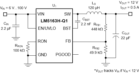
 Typical Application
 Typical Application
Efficiency, VOUT = 12 V