SNVSAU4C September 2018 – April 2024 LM5164
PRODUCTION DATA
- 1
- 1 Features
- 2 Applications
- 3 Description
- 4 Pin Configuration and Functions
- 5 Specifications
-
6 Detailed Description
- 6.1 Overview
- 6.2 Functional Block Diagram
- 6.3
Feature Description
- 6.3.1 Control Architecture
- 6.3.2 Internal VCC Regulator and Bootstrap Capacitor
- 6.3.3 Regulation Comparator
- 6.3.4 Internal Soft Start
- 6.3.5 On-Time Generator
- 6.3.6 Current Limit
- 6.3.7 N-Channel Buck Switch and Driver
- 6.3.8 Synchronous Rectifier
- 6.3.9 Enable/Undervoltage Lockout (EN/UVLO)
- 6.3.10 Power Good (PGOOD)
- 6.3.11 Thermal Protection
- 6.4 Device Functional Modes
- 7 Application and Implementation
- 8 Device and Documentation Support
- 9 Revision History
- 10Mechanical, Packaging, and Orderable Information
Package Options
Mechanical Data (Package|Pins)
- DDA|8
Thermal pad, mechanical data (Package|Pins)
- DDA|8
Orderable Information
3 Description
The LM5164 synchronous buck converter is designed to regulate over a wide input voltage range, minimizing the need for external surge suppression components. A minimum controllable on-time of 50ns facilitates large step-down conversion ratios, enabling the direct step-down from a 48V nominal input to low-voltage rails for reduced system complexity and solution cost. The LM5164 operates during input voltage dips as low as 6V, at nearly 100% duty cycle if needed, making the device an excellent choice for wide input supply range industrial and high cell count battery pack applications.
With integrated high-side and low-side power MOSFETs, the LM5164 delivers up to 1A of output current. A constant on-time (COT) control architecture provides nearly constant switching frequency with excellent load and line transient response. Additional features of the LM5164 include ultra-low IQ and diode emulation mode operation for high light-load efficiency, innovative peak and valley overcurrent protection, integrated VCC bias supply and bootstrap diode, precision enable and input UVLO, and thermal shutdown protection with automatic recovery. An open-drain PGOOD indicator provides sequencing, fault reporting, and output voltage monitoring.The LM5164 is available in a thermally-enhanced, 8-pin SO PowerPAD™ package. The 1.27mm pin pitch provides adequate spacing for high-voltage applications.
The LM5164 is available in a thermally-enhanced, 8-pin SO PowerPAD™ package. The device 1.27mm pin pitch provides adequate spacing for high-voltage applications.
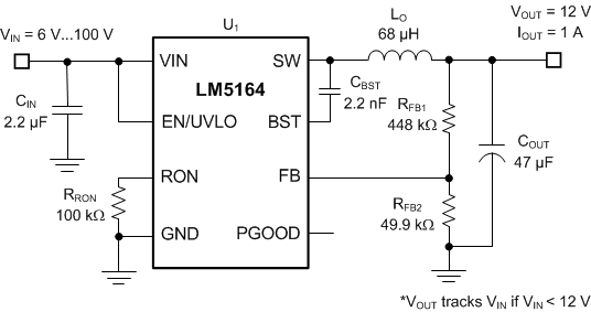
 Typical Application
 Typical Application
Efficiency, VOUT = 12V