SNVSAQ6D November 2016 – August 2021 LM5170-Q1
PRODUCTION DATA
- 1 Features
- 2 Applications
- 3 Description
- 4 Revision History
- 5 Description (continued)
- 6 Pin Configuration and Functions
- 7 Specifications
-
8 Detailed Description
- 8.1 Overview
- 8.2 Functional Block Diagram
- 8.3
Feature Description
- 8.3.1 Bias Supply (VCC, VCCA)
- 8.3.2 Undervoltage Lockout (UVLO) and Master Enable or Disable
- 8.3.3 High Voltage Input (VIN, VINX)
- 8.3.4 Current Sense Amplifier
- 8.3.5 Control Commands
- 8.3.6 Channel Current Monitor (IOUT1, IOUT2)
- 8.3.7 Cycle-by-Cycle Peak Current Limit (IPK)
- 8.3.8 Error Amplifier
- 8.3.9 Ramp Generator
- 8.3.10 Soft Start
- 8.3.11 Gate Drive Outputs, Dead Time Programming and Adaptive Dead Time (HO1, HO2, LO1, LO2, DT)
- 8.3.12 PWM Comparator
- 8.3.13 Oscillator (OSC)
- 8.3.14 Synchronization to an External Clock (SYNCIN, SYNCOUT)
- 8.3.15 Diode Emulation
- 8.3.16 Power MOSFET Failure Detection and Failure Protection (nFAULT, BRKG, BRKS)
- 8.3.17 Overvoltage Protection (OVPA, OVPB)
- 8.4 Device Functional Modes
- 8.5 Programming
-
9 Application and Implementation
- 9.1 Application Information
- 9.2
Typical Application
- 9.2.1
60-A, Dual-Phase, 48-V to 12-V Bidirectional Converter
- 9.2.1.1 Design Requirements
- 9.2.1.2
Detailed Design Procedure
- 9.2.1.2.1 Determining the Duty Cycle
- 9.2.1.2.2 Oscillator Programming
- 9.2.1.2.3 Power Inductor, RMS and Peak Currents
- 9.2.1.2.4 Current Sense (RCS)
- 9.2.1.2.5 Current Setting Limits (ISETA or ISETD)
- 9.2.1.2.6 Peak Current Limit
- 9.2.1.2.7 Power MOSFETS
- 9.2.1.2.8 Bias Supply
- 9.2.1.2.9 Boot Strap
- 9.2.1.2.10 RAMP Generators
- 9.2.1.2.11 OVP
- 9.2.1.2.12 Dead Time
- 9.2.1.2.13 IOUT Monitors
- 9.2.1.2.14 UVLO Pin Usage
- 9.2.1.2.15 VIN Pin Configuration
- 9.2.1.2.16 Loop Compensation
- 9.2.1.2.17 Soft Start
- 9.2.1.2.18 ISET Pins
- 9.2.1.3 Application Curves
- 9.2.1
60-A, Dual-Phase, 48-V to 12-V Bidirectional Converter
- 10Power Supply Recommendations
- 11Layout
- 12Device and Documentation Support
- 13Mechanical, Packaging, and Orderable Information
Package Options
Mechanical Data (Package|Pins)
- PHP|48
Thermal pad, mechanical data (Package|Pins)
- PHP|48
Orderable Information
8.3.16.2 Nominal Circuit Breaker Function
If the failure detection function is enabled, which also implies the circuit breaker being controlled by the LM5170-Q1, the LM5170-Q1 will perform a MOSFET failure detection during start-up. The detection starts after the UVLO is pulled higher than 2.5 V and VCC above 8.5 V. The detection operation lasts for 2 to 3 ms. During the detection, the LM5170-Q1 checks the high-side and low-side MOSFETs of both channels as well as the circuit breaker MOSFETs to see if any of them has drain-to-source shorted. If no failure is detected, a 330-µA current source at the BRKG pin is turned on to charge up the breaker MOSFET gates. When the BRKG to BRKS voltage rises above 8.5 V, the LM5170-Q1 enters standby mode, waiting for the EN1 and EN2 commands to operate in power delivery mode. The voltage across BRKG and BRKS is internally clamped to 12 V, preventing overvoltage stress on the breaker MOSFET gates.
If a failure of any MOSFET is detected, the LM5170-Q1 immediately pulls the nFAULT pin low, and keeps the LM5170-Q1 in a latched shutdown mode, thereby preventing catastrophic failure.
The nFAULT pin can also be externally pulled low during normal operation and the LM5170-Q1 immediately turns off the circuit breaker and stays in a latched shutdown. There is a 2-µs glitch filter at the nFAULT pin to prevent errant shutdown by possible noises at the nFAULT pin.
To release the nFAULT shutdown latch, it requires the UVLO pin to be externally forced below 1.25 V, or VCC is below 8 V.
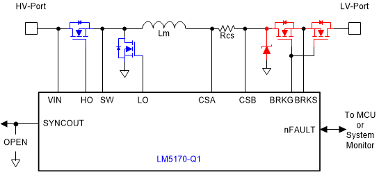
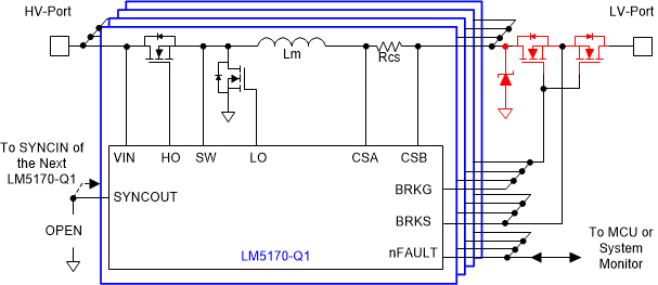
Figure 8-15 and Figure 8-16 show two ways to use the circuit breaker function. A TVS is recommended to prevent surge voltage when the circuit breaker is turned off during operation.
The BRKG 330-µA current source is powered by the VIN pin, or the HV-Port. Therefore, the differential voltage between the HV-Port and LV-Port should be greater than 10 V to ensure that BRKG to BRKS voltage can establish > 8.5 V and allow the LM5170-Q1 to enter power delivery mode. The BRKG to BRKS voltage is internally clamped to 12 V if the differential voltage of the two ports is greater.
The load dump transient at the LV-Port may raise the rail voltage and reduce the differential voltage of the two ports to below 10 V. To maintain the circuit breaker to be closed during the transient, TI recommends adding a 1-nF to 10-nF capacitor across BRKG and BRKS to hold the gate voltage during the transient.
Note that the BRKG 330-µA current source will always be turned on once the LM5170 starts up. If the failure detection mode is deactivated, the LM5170-Q1 will also skip checking the BRKG to BRKS votlage condition. Therefore, the circuit breaker can still be controlled by the LM5170-Q1 even if the failure detection is deactivated. If the steady-state differential voltage between the HV-Port and LV-Port is less than 10 V during power up, TI does not recommend the user to activate the failure detection function. Also, if the differential voltage is less than 8 V, TI recommends not to use the circuit breaker function of the LM5170-Q1 at all.
 Figure 8-15 Controlling Dual-Channel Circuit Breaker for MOSFET Failure Protection
 Figure 8-16 Controlling System Level Circuit Breaker for MOSFET Failure Protection
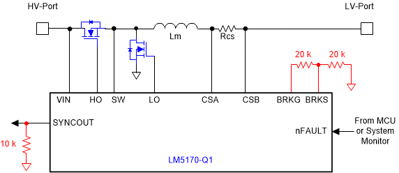
 Figure 8-17 Circuit Breaker Function Disabled