SNVSC75A April 2023 – July 2024 LM5171-Q1
ADVANCE INFORMATION
- 1
- 1 Features
- 2 Applications
- 3 Description
- 4 Pin Configuration and Functions
- 5 Specifications
-
6 Detailed Description
- 6.1 Overview
- 6.2 Functional Block Diagram
- 6.3
Feature Description
- 6.3.1 Bias Supplies and Voltage Reference (VCC, VDD, and VREF)
- 6.3.2 Undervoltage Lockout (UVLO) and Controller Enable or Disable
- 6.3.3 High Voltage Inputs (HV1, HV2)
- 6.3.4 Current Sense Amplifier
- 6.3.5 Control Commands
- 6.3.6 Channel Current Monitor (IMON1, IMON2)
- 6.3.7 Cycle-by-Cycle Peak Current Limit (IPK)
- 6.3.8 Inner Current Loop Error Amplifier
- 6.3.9 Outer Voltage Loop Error Amplifier
- 6.3.10 Soft Start, Diode Emulation, and Forced PWM Control (SS/DEM1 and SS/DEM2)
- 6.3.11 Gate Drive Outputs, Dead Time Programming and Adaptive Dead Time (HO1, HO2, LO1, LO2, DT/SD)
- 6.3.12 Emergency Latched Shutdown (DT/SD)
- 6.3.13 PWM Comparator
- 6.3.14 Oscillator (OSC)
- 6.3.15 Synchronization to an External Clock (SYNCI, SYNCO)
- 6.3.16 Overvoltage Protection (OVP)
- 6.3.17 Multiphase Configurations (SYNCO, OPT)
- 6.3.18 Thermal Shutdown
- 6.4 Programming
- 6.5
Registers
- 6.5.1 I2C Serial Interface
- 6.5.2 I2C Bus Operation
- 6.5.3 Clock Stretching
- 6.5.4 Data Transfer Formats
- 6.5.5 Single READ From a Defined Register Address
- 6.5.6 Sequential READ Starting From a Defined Register Address
- 6.5.7 Single WRITE to a Defined Register Address
- 6.5.8 Sequential WRITE Starting From A Defined Register Address
- 6.5.9 REGFIELD Registers
-
7 Application and Implementation
- 7.1 Application Information
- 7.2
Typical Application
- 7.2.1
60A, Dual-Phase, 48V to 12V Bidirectional Converter
- 7.2.1.1 Design Requirements
- 7.2.1.2
Detailed Design Procedure
- 7.2.1.2.1 Determining the Duty Cycle
- 7.2.1.2.2 Oscillator Programming
- 7.2.1.2.3 Power Inductor, RMS and Peak Currents
- 7.2.1.2.4 Current Sense (RCS)
- 7.2.1.2.5 Current Setting Limits (ISETx)
- 7.2.1.2.6 Peak Current Limit
- 7.2.1.2.7 Power MOSFETS
- 7.2.1.2.8 Bias Supply
- 7.2.1.2.9 Boot Strap
- 7.2.1.2.10 OVP
- 7.2.1.2.11 Dead Time
- 7.2.1.2.12 Channel Current Monitor (IMONx)
- 7.2.1.2.13 UVLO Pin Usage
- 7.2.1.2.14 HVx Pin Configuration
- 7.2.1.2.15 Loop Compensation
- 7.2.1.2.16 Soft Start
- 7.2.1.2.17 PWM to ISET Pins
- 7.2.1.2.18 Proper Termination of Unused Pins
- 7.2.1.3 Application Curves
- 7.2.1
60A, Dual-Phase, 48V to 12V Bidirectional Converter
- 7.3 Power Supply Recommendations
- 7.4 Layout
- 8 Device and Documentation Support
- 9 Revision History
- 10Mechanical, Packaging, and Orderable Information
Package Options
Mechanical Data (Package|Pins)
- PHP|48
Thermal pad, mechanical data (Package|Pins)
- PHP|48
Orderable Information
6.4.2 UVLO Programming
The UVLO pin is the enable pin of the LM5171-Q1 controller. It can be directly controlled by an external control unit like an MCU.
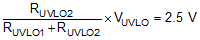
Nevertheless, the UVLO pin can also fulfill the undervoltage lockout function of a particular power rail. The rail can be either the HV-Port, or the LV-Port, or VCC. Use a resistor divider to set the UVLO threshold, as shown in Figure 6-31. The divider must satisfy Equation 20:
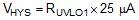
The UVLO hysteresis is accomplished with an internal 25-μA current source. When UVLO > 2.5 V, the current source is activated to instantly raise the voltage at the UVLO pin. When the UVLO pin voltage falls below the 2.5-V threshold the current source is turned off, causing the voltage at the UVLO pin to fall. The UVLO hysteresis is determined by Equation 21:
An optional ceramic capacitor CUVLO can be placed in parallel with RUVLO2 to improve the noise immunity. CUVLO is usually between 1 nF to 10 nF. A large CUVLO may cause excessive delay to respond to a real UVLO event.
If Equation 21 does not provide adequate hysteresis voltage, the user can add RUVLO3 as shown in Figure 6-32. The hysteresis voltage is thus given by Equation 22:
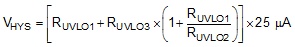
 Figure 6-31 UVLO Programming
 Figure 6-32 UVLO With Additional Hysteresis Programming