SNVSCL2 December 2024 LM51770
PRODUCTION DATA
- 1
- 1 Features
- 2 Applications
- 3 Description
- 4 Device Comparison
- 5 Pin Configuration and Functions
- 6 Specifications
- 7 Parameter Measurement Information
-
8 Detailed Description
- 8.1 Overview
- 8.2 Functional Block Diagram
- 8.3
Feature Description
- 8.3.1 Power-On Reset (POR System)
- 8.3.2 Buck-Boost Control Scheme
- 8.3.3 Power Save Mode
- 8.3.4 Supply Voltage Selection – VMAX Switch
- 8.3.5 Enable and Undervoltage Lockout
- 8.3.6 Oscillator Frequency Selection
- 8.3.7 Frequency Synchronization
- 8.3.8 Voltage Regulation Loop
- 8.3.9 Output Voltage Tracking
- 8.3.10 Slope Compensation
- 8.3.11 Configurable Soft Start
- 8.3.12 Peak Current Sensor
- 8.3.13 Current Monitoring and Current Limit Control Loop
- 8.3.14 Short Circuit - Hiccup Protection
- 8.3.15 nFLT Pin and Protections
- 8.3.16 Device Configuration Pin
- 8.3.17 Dual Random Spread Spectrum – DRSS
- 8.3.18 Gate Driver
- 8.4 Device Functional Modes
-
9 Application and Implementation
- 9.1 Application Information
- 9.2
Typical Application
- 9.2.1
Detailed Design Procedure
- 9.2.1.1 Custom Design with WEBENCH Tools
- 9.2.1.2 Frequency
- 9.2.1.3 Feedback Divider
- 9.2.1.4 Inductor and Current Sense Resistor Selection
- 9.2.1.5 Slope Compensation
- 9.2.1.6 Output Capacitor
- 9.2.1.7 Input Capacitor
- 9.2.1.8 UVLO Divider
- 9.2.1.9 Soft-Start Capacitor
- 9.2.1.10 MOSFETs QH1 and QL1
- 9.2.1.11 MOSFETs QH2 and QL2
- 9.2.1.12 Frequency Compensation
- 9.2.1.13 External Component Selection
- 9.2.2 Application Curves
- 9.2.1
Detailed Design Procedure
- 10Power Supply Recommendations
- 11Layout
- 12Device and Documentation Support
- 13Revision History
- 14Mechanical, Packaging, and Orderable Information
Package Options
Mechanical Data (Package|Pins)
- DCP|38
Thermal pad, mechanical data (Package|Pins)
- DCP|38
Orderable Information
8.3.15 nFLT Pin and Protections
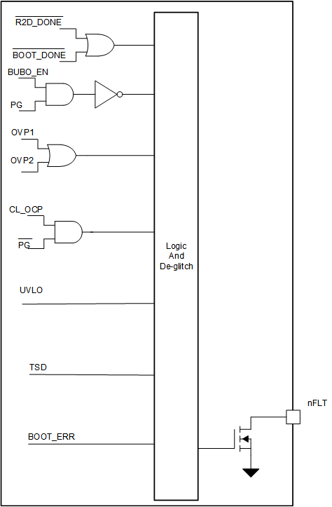
The open-drain nFLT ouput directly follows the input signals of monitoring features. For instance if the power good flag triggers because the output voltage is falling below the power good threshold the nFLT pins pulls low. After a power-cycle of the device or in case the internal failure signal disappears the nFLT pin will go back to HighZ. The input signals to the nFLT pin are digitally de-glitched. Due to this the maximum reaction time of the FLT pin is given by td(nFLT-PIN)
 Figure 8-19 Functional Block Diagram nFLT-pin Logic
 Thermal Shutdown (TSD)
To avoid the case of a thermal damage of the device the die temperature of the die is monitored. The device will stop operation once the sensed temperature rises over the thermal shutdown threshold. After the temperature drops below the thermal shutdown hysteresis the TSD signal goes back to normal and the converter will return to normal operation according to the main FSM definition.
Over Current or Short Circuit Protection
The device features a hiccup mode short circuit protection to avoid excessive power dissipation in the die or at the fault of the application in the System. The OCP triggers if the peak current sensing voltage between CSA-pin and CSB-pin is exceeded.
The protection feature will stop and restart the converter operation in case of a short is event is detected.
Output Over Voltage Protection 1 (OVP1)
This over voltage protection monitors the voltage of the FB-pin.
As this threshold is referenced to the V(REF) the OVP1 continues its operation even if of tracking features has changed the Vo target value.
The converter maintains in regulation even the OVP1 threshold triggers.
The OVP1 is disabled during PSM to avoid additional leakage current. The OVP signal gets masked to avoid that a fault is indicated from this signal during the PSM operation.
This protection is disabled during the soft-start procedure.
Output Over Voltage protection 2 (OVP2)
This feature shall avoid any damage to the device in case the external feedback pin is not working properly i.e. is shorted to GND
If the output voltage threshold VT+(OVP2) is reached on the VOUT-pin the buck-boost core logic disables the converter power stage and enters a high impedance state at the switch nodes. If the output voltage falls back under this threshold the convert operation is resumed.
Input Voltage Protection (IVP)
The input over voltage protection is part of the converter core modulation scheme. The IVP avoids any damage to the device in case the current flows from the output to the input and the input source can not sink current e.g. there is a diode in the supply path. If the converter forced PWM mode is active the current can go negative until the sink current limit. Once the input voltage threshold VT+(IVP) is reach on the VIN-pin the protection disables the forced PWM mode and only allows current to flow from VIN to VOUT. After the input voltage drops under the input voltage protection threshold, the fPWM mode activates again.
Power Good
The device features a power good detection. The FB pin voltages gets contentiously monitors. If the sensed voltage drops below the PG falling threshold the signal is pulling low the nFLT pin.
This protection is disabled during the soft-start procedure.
Boot-strap Under Voltage Protection
The high side supply voltage for the gate driver are monitored by an UVLO comparator (BST_UV). This comparator monitors the differential voltage between SWx pin and HBx pin. If the measured voltage drops below VTH-(BST_UV) the converter stops operation
Boot-strap Over Voltage Clamp
To protect the internal gate driver circuit the external FET gates and the internal circuit features an over voltage clamp. If the voltage goes above VTH(BST_OV) the linear regulator sinks a current from HBx pin to SWx-pin as long as the voltage is above the threshold.