SNVSCL2 December 2024 LM51770
PRODUCTION DATA
- 1
- 1 Features
- 2 Applications
- 3 Description
- 4 Device Comparison
- 5 Pin Configuration and Functions
- 6 Specifications
- 7 Parameter Measurement Information
-
8 Detailed Description
- 8.1 Overview
- 8.2 Functional Block Diagram
- 8.3
Feature Description
- 8.3.1 Power-On Reset (POR System)
- 8.3.2 Buck-Boost Control Scheme
- 8.3.3 Power Save Mode
- 8.3.4 Supply Voltage Selection – VMAX Switch
- 8.3.5 Enable and Undervoltage Lockout
- 8.3.6 Oscillator Frequency Selection
- 8.3.7 Frequency Synchronization
- 8.3.8 Voltage Regulation Loop
- 8.3.9 Output Voltage Tracking
- 8.3.10 Slope Compensation
- 8.3.11 Configurable Soft Start
- 8.3.12 Peak Current Sensor
- 8.3.13 Current Monitoring and Current Limit Control Loop
- 8.3.14 Short Circuit - Hiccup Protection
- 8.3.15 nFLT Pin and Protections
- 8.3.16 Device Configuration Pin
- 8.3.17 Dual Random Spread Spectrum – DRSS
- 8.3.18 Gate Driver
- 8.4 Device Functional Modes
-
9 Application and Implementation
- 9.1 Application Information
- 9.2
Typical Application
- 9.2.1
Detailed Design Procedure
- 9.2.1.1 Custom Design with WEBENCH Tools
- 9.2.1.2 Frequency
- 9.2.1.3 Feedback Divider
- 9.2.1.4 Inductor and Current Sense Resistor Selection
- 9.2.1.5 Slope Compensation
- 9.2.1.6 Output Capacitor
- 9.2.1.7 Input Capacitor
- 9.2.1.8 UVLO Divider
- 9.2.1.9 Soft-Start Capacitor
- 9.2.1.10 MOSFETs QH1 and QL1
- 9.2.1.11 MOSFETs QH2 and QL2
- 9.2.1.12 Frequency Compensation
- 9.2.1.13 External Component Selection
- 9.2.2 Application Curves
- 9.2.1
Detailed Design Procedure
- 10Power Supply Recommendations
- 11Layout
- 12Device and Documentation Support
- 13Revision History
- 14Mechanical, Packaging, and Orderable Information
Package Options
Mechanical Data (Package|Pins)
- DCP|38
Thermal pad, mechanical data (Package|Pins)
- DCP|38
Orderable Information
9.2.2 Application Curves
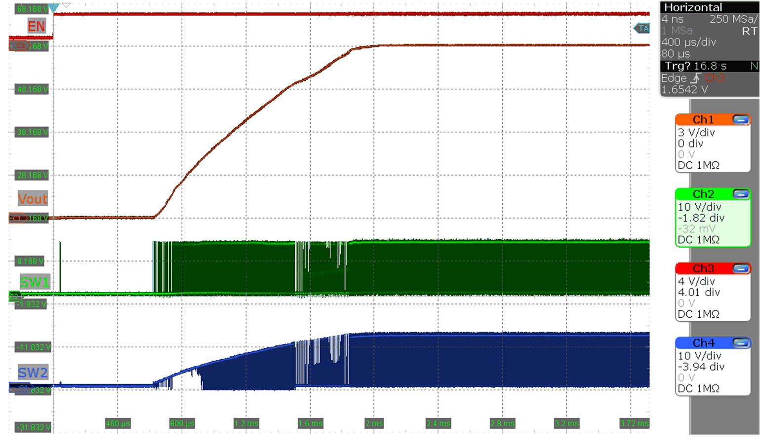 Figure 9-2 Start-up waveform standby to active operation
 (MODE = V(VCC), Vo = 12 V, Io = 0 A, V(VIN) = 12 V)
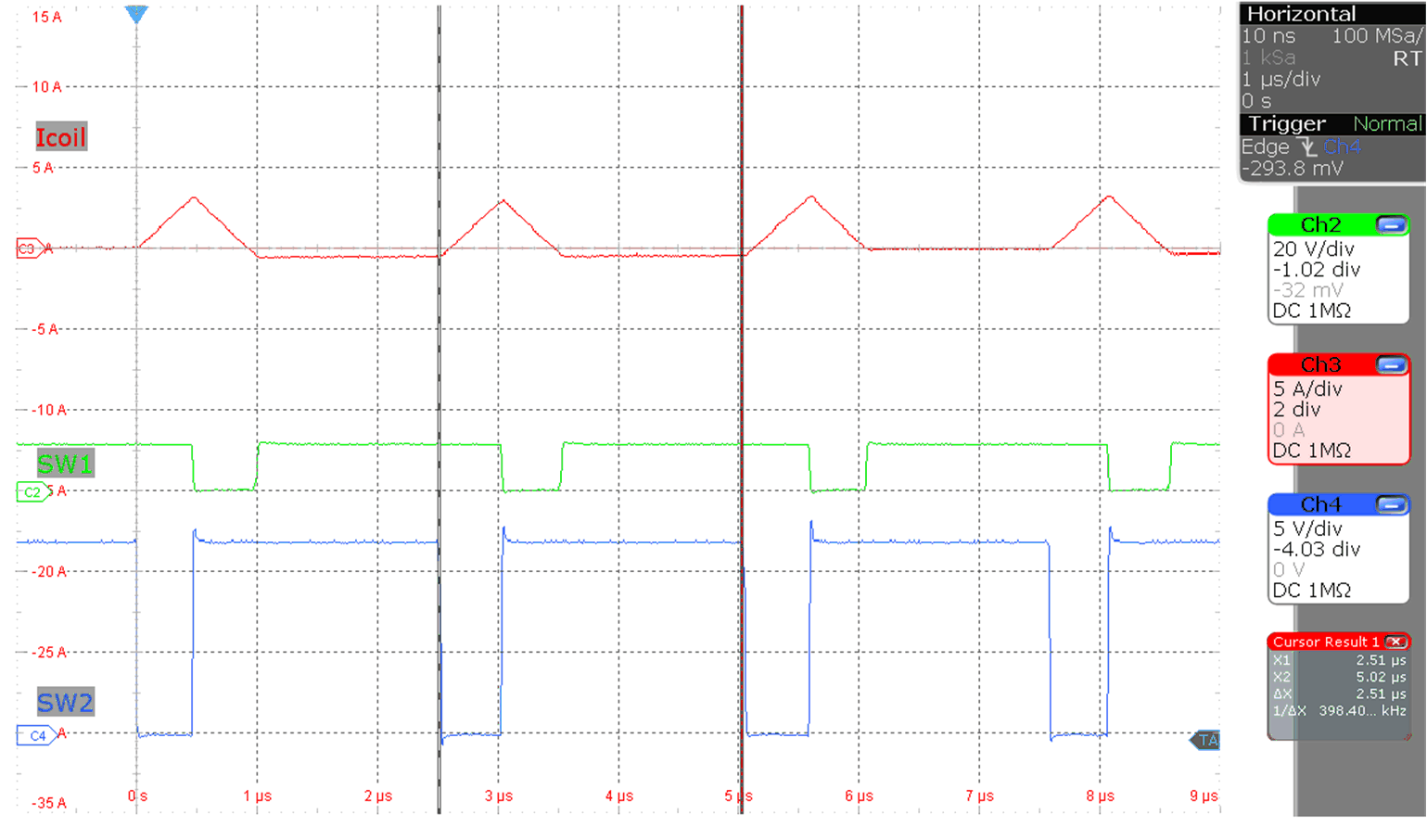 Figure 9-4 Inductor current
buck-boost operation
 (MODE = V(VCC), Vo = 12 V, Io = 0 A, V(VIN) = 12 V)
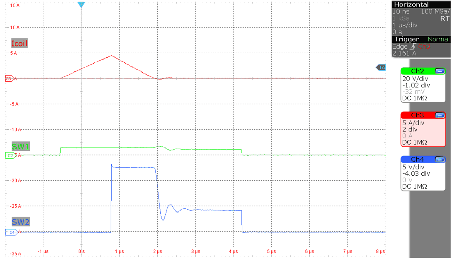 Figure 9-6 Inductor current boost
operation
 (MODE = 0 V, Vo = 12 V, Io = 10 mA, V(VIN) = 6 V)
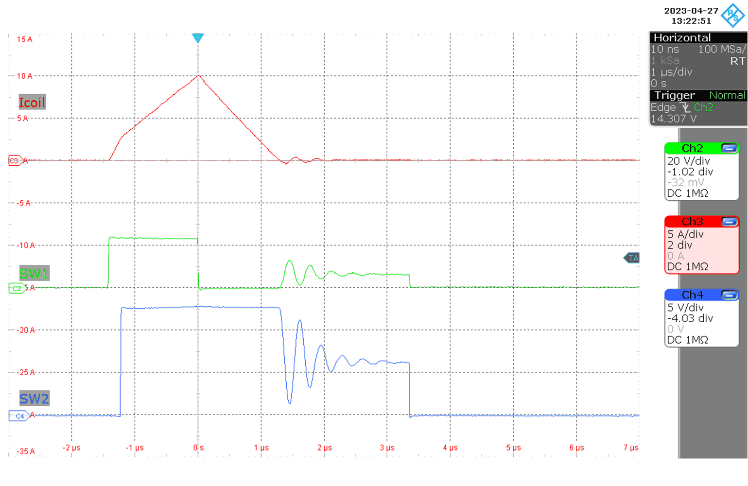 Figure 9-8 Inductor current buck
operation
 (MODE = 0 V, Vo = 12 V, Io = 10 mA, V(VIN) = 24 V)
 Figure 9-10 Efficiency Versus IO
(MODE = 0V Vo = 12 V)
 Figure 9-12 Efficiency Versus IO in Boost Mode
(VIN = 5 V, Vo = 12 V)
 Figure 9-14 Efficiency Versus IO in Buck Mode
VIN = 24 V, Vo = 12 V)
 Figure 9-3 Inductor current boost
operation
 (MODE = V(VCC), Vo = 12 V, Io = 0 A, V(VIN) = 6 V)
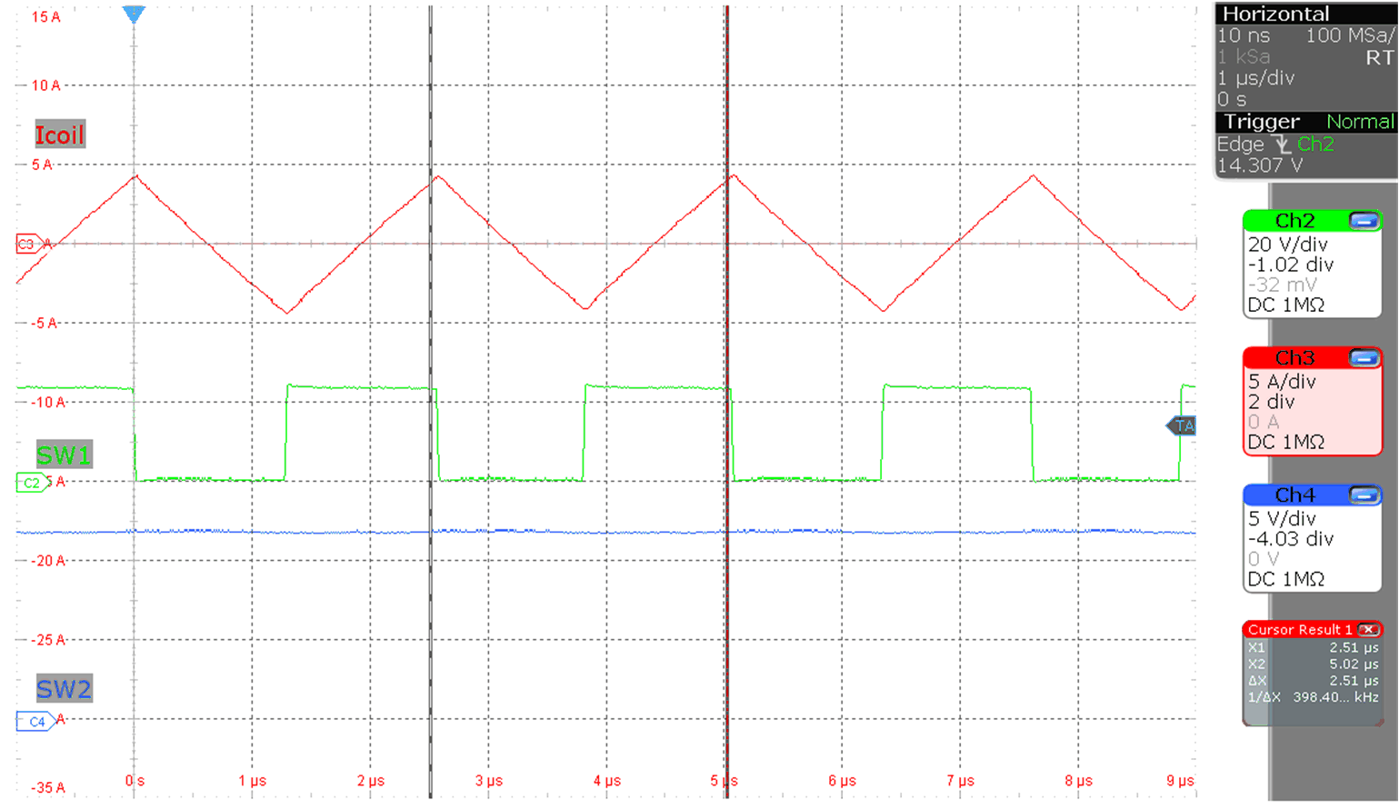 Figure 9-5 Inductor current buck
operation
 (MODE = V(VCC), Vo = 12 V, Io = 0 A, V(VIN) = 24 V)
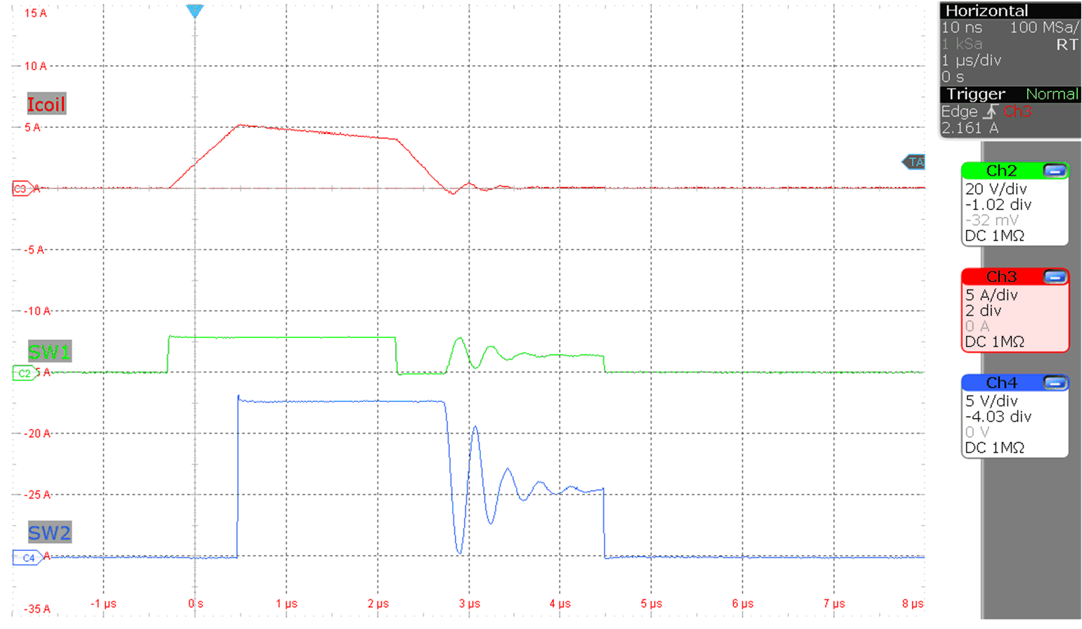 Figure 9-7 Inductor current
buck-boost operation
 (MODE = 0 V, Vo = 12 V, Io = 10 mA, V(VIN) = 12 V)
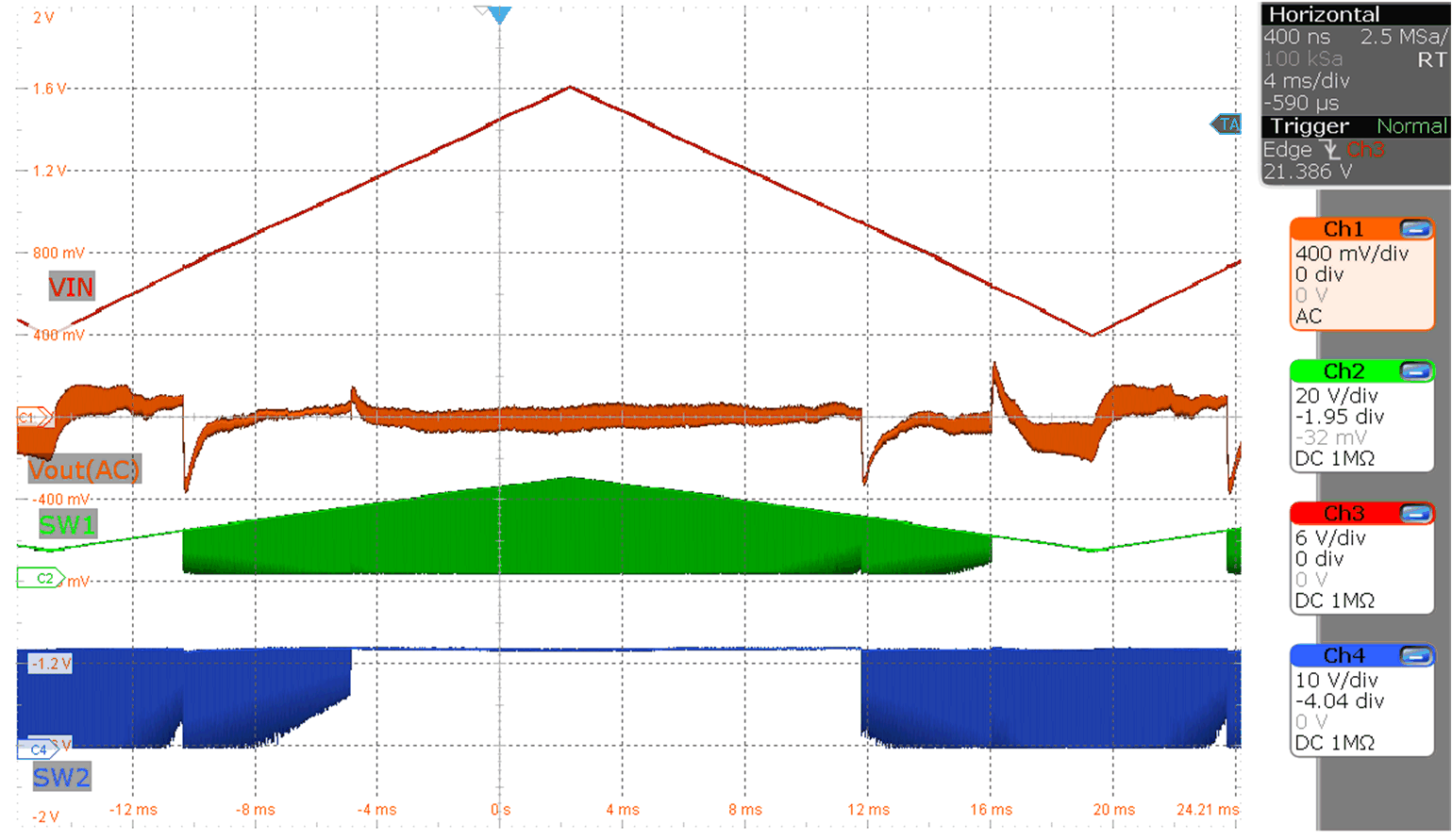 Figure 9-9 Input voltage ramp from 6V
to 24V
 (MODE = V(VCC), Vo = 12 V, Io = 6A
 Figure 9-11 Efficiency Versus IO
(MODE = VCC Vo = 12 V)
 Figure 9-13 Efficiency Versus IO in Buck-Boost Mode
VIN = 12 V, Vo = 12 V)
 Figure 9-15 Efficiency Versus VIN
(Vo = 24 V, IO = 5 A)