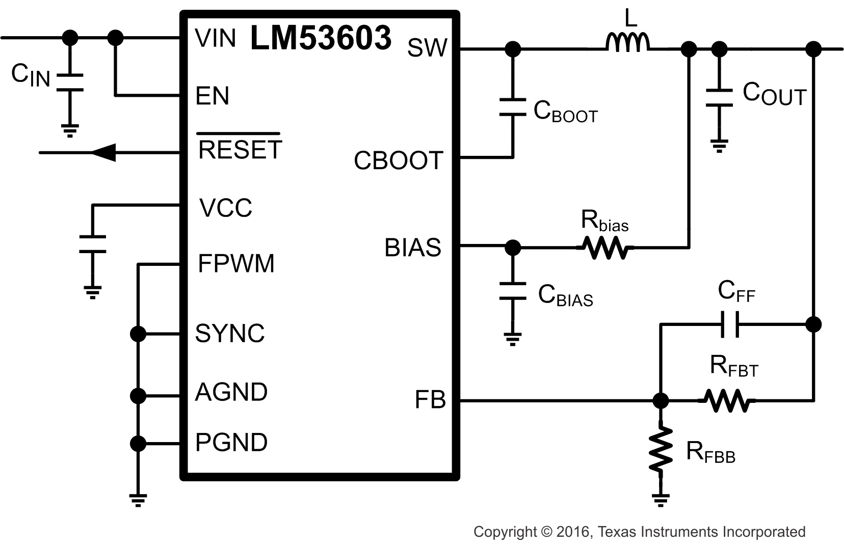
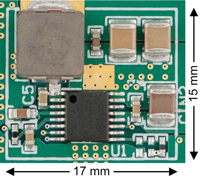
The LM53603 and LM53602 buck regulators are specifically designed for 12-V industrial and automotive applications, providing an adjustable output voltage from 3.3 V to 10 V at 3 A or 2 A, from an input voltage of up to 36 V. Advanced high-speed circuitry allows the device to regulate from an input of up to 20 V, while providing an output of 5 V at a switching frequency of 2.1 MHz. The innovative architecture allows the device to regulate a 3.3-V output from an input voltage of only 3.5 V. All aspects of this product are optimized for the industrial and automotive customer. An input voltage range up to 36 V, with transient tolerance up to 42 V, eases input surge protection design. An open-drain reset output, with filtering and delay, provides a true indication of system status. This feature negates the requirement for an additional supervisory component, saving cost and board space. Seamless transition between PWM and PFM modes, along with a no-load operating current of only 24 µA, ensures high efficiency and superior transient response at all loads.
PART NUMBER | PACKAGE | BODY SIZE (NOM) |
---|---|---|
LM53603 LM53602 |
HTSSOP (16) | 5.00 mm x 4.40 mm |
DATE | REVISION | NOTES |
---|---|---|
November 2016 | * | Initial release. |
PART NUMBER(1) | OUTPUT VOLTAGE | MAXIMUM OUTPUT CURRENT | PACKAGE QTY |
---|---|---|---|
LM53603AMPWPR | Adjustable | 3 A | 2000 |
LM53603AMPWPT | Adjustable | 3 A | 250 |
LM53602AMPWPR | Adjustable | 2 A | 2000 |
LM53602AMPWPT | Adjustable | 2 A | 250 |
PIN | I/O(1) | DESCRIPTION | |
---|---|---|---|
NO. | NAME | ||
1, 2 | SW | P | Regulator switch node. Connect to power inductor. Connect pins 1 and 2 directly together at the PCB. |
3 | CBOOT | P | Bootstrap supply input for gate drivers. Connect a high-quality, 470-nF capacitor from this pin to SW. |
4 | VCC | O | Internal 3.15-V regulator output. Used as supply to internal control circuits. Do not connect to any external loads. Can be used as logic supply for control inputs. Connect a high-quality, 3.3-µF capacitor from this pin to GND. |
5 | BIAS | P | Input to internal voltage regulator. Connect to output voltage point. Do not ground. Connect a high-quality, 0.1-µF capacitor from this pin to GND. |
6 | SYNC | I | Synchronization input to regulator. Used to synchronize the regulator switching frequency to the system clock. When not used connect to GND; do not float. |
7 | FPWM | I | Mode control input to regulator. High = forced PWM (FPWM). Low = auto mode; automatic transition between PFM and PWM. Do not float. |
8 | RESET | O | Open-drain reset output. Connect to suitable voltage supply through a current limiting resistor. High = power OK. Low = fault. RESET goes low when EN = low. |
9 | FB | I | Feedback input to regulator. Connect to output voltage sense point for fixed 5-V and 3.3-V output. Connect to feedback divider tap point for ADJ option. Do not float or ground. |
10 | AGND | G | Analog ground for regulator and system. All electrical parameters are measured with respect to this pin. Connect to EP and PGND on PCB. |
11 | EN | I | Enable input to the regulator. High = ON. Low = OFF. Can be connected directly to VIN. Do not float. |
12, 13 | VIN | P | Input supply to the regulator. Connect a high-quality bypass capacitor(s) from this pin to PGND. Connect pins 12 and 13 directly together at the PCB. |
14 | N/C | — | This pin has no connection to the device. |
15, 16 | PGND | G | Power ground to internal low-side MOSFET. Connect to AGND and system ground. Connect pins 15 and 16 directly together at the PCB. |
17 | EP | G | Exposed die attach paddle. Connect to ground plane for adequate heat sinking and noise reduction. |
PARAMETER | MIN | MAX | UNIT |
---|---|---|---|
VIN to AGND, PGND(2) | –0.3 | 40 | V |
SW to AGND, PGND(3) | –0.3 | VIN + 0.3 | V |
CBOOT to SW | –0.3 | 3.6 | V |
EN to AGND, PGND(2) | –0.3 | 40 | V |
BIAS to AGND, PGND | –0.3 | 16 | V |
FB to AGND, PGND : fixed 5 V and 3.3 V | –0.3 | 16 | V |
FB to AGND, PGND : ADJ | –0.3 | 5.5 | V |
RESET to AGND, PGND | –0.3 | 8 | V |
SYNC, FPWM, to AGND, PGND | –0.3 | 5.5 | V |
VCC to AGND, PGND | –0.3 | 4.2 | V |
RESET pin current(4) | –0.1 | 1.2 | mA |
AGND to PGND(5) | –0.3 | 0.3 | V |
Storage temperature, Tstg | –40 | 150 | °C |
VALUE | UNIT | ||||
---|---|---|---|---|---|
V(ESD) | Electrostatic discharge | Human-body model (HBM), per ANSI/ESDA/JEDEC JS-001(1) | Pins 1, 2, 3, 12, 13, | ±1500 | V |
Pins 11, 5, 8, 9, 6, 7, 4 | ±2500 | ||||
Charged-device model (CDM), per JEDEC specification JESD22-C101(2) | Pins 3, 4, 5, 6, 7, 11, 12 and 13 | ±750 | |||
Pins 1, 2, 8, 9, 15 and 16 | ±500 |
MIN | NOM | MAX | UNIT | ||
---|---|---|---|---|---|
Input voltage(3) | 3.9 | 36 | V | ||
Output voltage : fixed 5 V(1) | 0 | 5 | V | ||
Output voltage : fixed 3.3 V(1) | 0 | 3.3 | V | ||
Output voltage adjustment range: ADJ(1)(2) | 3.3 | 10 | V | ||
Output current for LM53603 | 0 | 3 | A | ||
Output current for LM53602 | 0 | 2 | A | ||
RESET pin current | 0 | 1 | mA | ||
Operating junction temperature(4) | –40 | 150 | °C |
THERMAL METRIC(1) | LM53603, LM53602 | UNIT | |
---|---|---|---|
PWP (HTSSOP) | |||
16 PINS | |||
RθJA | Junction-to-ambient thermal resistance | 42.5 | °C/W |
RθJC(top) | Junction-to-case (top) thermal resistance | 22.6 | °C/W |
RθJB | Junction-to-board thermal resistance | 16.2 | °C/W |
ψJT | Junction-to-top characterization parameter | 0.6 | °C/W |
ψJB | Junction-to-board characterization parameter | 16.0 | °C/W |
RθJC(bot) | Junction-to-case (bottom) thermal resistance | 1.1 | °C/W |
PARAMETER | TEST CONDITIONS | MIN(1) | TYP | MAX(1) | UNIT | |
---|---|---|---|---|---|---|
VFB | Initial reference voltage accuracy for 5-V and 3.3-V options | VIN = 3.8 V to 36 V, FPWM, TJ = 25°C |
–1% | 1% | ||
VIN = 3.8 V to 36 V, FPWM | –1.25% | 1.25% | ||||
VREF | Reference voltage for ADJ option | VIN = 3.8 V to 36 V, FPWM, TJ = 25°C |
0.993 | 1 | 1.007 | V |
VIN = 3.8 V to 36 V, FPWM, TJ = –40°C to 125°C |
0.99 | 1 | 1.01 | |||
VIN-operate | Minimum input voltage to operate(2) | Rising | 3.2 | 3.95 | V | |
Falling | 2.9 | 3.55 | ||||
Hysteresis, below | 0.34 | |||||
IQ | Operating quiescent current; measured at VIN pin(3)(4) | VBIAS = 5 V, TJ = –40°C to 125°C |
8 | 13 | µA | |
ISD | Shutdown quiescent current; measured at VIN pin | EN ≤ 0.4 V, TJ = 25°C | 1.7 | µA | ||
EN ≤ 0.4 V, TJ = 125°C | 3.5 | |||||
IB | Current into the BIAS pin(4) | VBIAS = 5 V, FPWM = 3.3 V | 47 | 78 | µA | |
IEN | Current into EN pin | VIN = VEN = 13.5 V | 2.3 | µA | ||
IFB | Bias current into FB pin | ADJ option | 10 | nA | ||
VRESET | RESET upper threshold voltage | Rising, % of nominal Vout | 105% | 107% | 110% | |
RESET lower threshold voltage | Falling, % of nominal Vout | 92% | 94% | 96.5% | ||
RESET lower threshold voltage with respect to output voltage | Falling, % actual Vout | 94.5% | 95.7% | |||
VRESET-Hyst | RESET hysteresis as a percent of output voltage set point | 1.5% | ||||
VMIN | Minimum input voltage for proper RESET function | 50-µA pullup to RESET pin, VEN = 0 V, TJ = 25°C |
1.5 | V | ||
VOL | Low level RESET pin output voltage | 50-µA pullup to RESET pin, Vin = 1.5 V, EN = 0 V | 0.4 | V | ||
0.5-mA pullup to RESET pin, Vin = 13.5 V, EN = 0 V | 0.4 | |||||
1-mA pullup to RESET pin, Vin = 13.5 V, EN = 3.3 V | 0.4 | |||||
VEN | Enable input threshold voltage | Rising | 1.7 | 2 | V | |
Hysteresis, below | 0.45 | 0.55 | ||||
VEN-off | Enable input threshold for full shutdown(5) | EN input voltage required for complete shutdown of the regulator, falling. | 0.8 | V | ||
VLOGIC | Logic input levels on FPWM and SYNC pins | VIH | 1.5 | V | ||
VIL | 0.4 | |||||
IHS | High-side switch current limit | LM53603 | 4.5 | 6.2 | A | |
LM53602 | 2.4 | 4.4 | ||||
ILS | Low-side switch current limit(6) | LM53603 | 3 | 3.6 | 4.3 | A |
LM53602 | 2 | 2.4 | 2.8 | |||
IZC | Zero-cross current limit | FPWM = 0 V | –0.02 | A | ||
INEG | Negative current limit | FPWM = 3.3 V | –1.5 | A | ||
Rdson | Power switch on-resistance | High-side MOSFET resistance | 135 | 290 | mΩ | |
Low-side MOSFET resistance | 60 | 125 | ||||
FSW | Switching frequency | VIN = 3.8 V to 18 V | 1.85 | 2.1 | 2.35 | MHz |
VIN = 36 V | 1.2 | |||||
FSYNC | Synchronizing frequency range | 1.9 | 2.1 | 2.3 | MHz | |
VCC | Internal VCC voltage | VBIAS = 3.3 V | 3.15 | V | ||
TSD | Thermal shutdown thresholds | Rising | 162 | 178 | °C | |
Hysteresis, below | 18 |
PARAMETER | TEST CONDITIONS | MIN | TYP | MAX | UNIT | |
---|---|---|---|---|---|---|
VIN-MIN | Minimum input voltage for Vout to stay within ±2% of regulation(2) | VOUT = 3.3 V, IOUT = 3 A | 3.9 | V | ||
VOUT = 3.3 V, IOUT = 1 A | 3.55 | |||||
Regulation | Line Regulation | VOUT = 5 V, VIN = 8 V to 36 V, IOUT = 3 A | 7 | mV | ||
VOUT = 3.3 V, VIN = 6 V to 36 V, IOUT = 3 A | 5 | |||||
Load Regulation : Auto Mode | VOUT = 5 V, VIN = 12 V, IOUT = 10 µA to 3 A | 77 | mV | |||
VOUT = 3.3 V, VIN = 12 V, IOUT = 10 µA to 3 A | 53 | |||||
Load Regulation : FPWM Mode | VOUT = 5 V, VIN = 12 V, IOUT = 10 µA to 3 A | 12 | mV | |||
VOUT = 3.3 V, VIN = 12 V, IOUT = 10 µA to 3 A | 9 | |||||
ISUPPLY | Input supply current when in regulation(1) | VIN = 13.5 V, VOUT = 3.3 V, IOUT = 0 A | 24 | µA | ||
VIN = 13.5 V, VOUT = 5 V, IOUT = 0 A | 34 | |||||
VDROP | Dropout voltage (VIN – VOUT) | 5-V Option:
VOUT = 4.95 V, IOUT = 3 A, FSW < 1.85 MHz |
0.7 | V | ||
5-V Option:
VOUT = 5 V, IOUT = 3 A, FSW = 1.85 MHz |
1.8 | |||||
3.3-V Option:
VOUT = 3.27 V, IOUT = 3 A, FSW < 1.85 MHz |
0.65 | |||||
3.3-V Option:
VOUT = 3.3 V, IOUT = 3 A, FSW = 1.85 MHz |
1.8 |
MIN | NOM | MAX | UNIT | ||
---|---|---|---|---|---|
TON | Minimum switch on-time, VIN = 20 V | 50 | 80 | ns | |
TOFF | Minimum switch off-time, VIN = 3.8 V | 125 | 200 | ns | |
TRESET-act | Delay time to RESET high signal | 2 | 3 | 4 | ms |
TRESET-filter | Glitch filter time for RESET function | 12 | 25 | 45 | µs |
TSS | Soft-start time | 1 | 2 | 3 | ms |
TEN | Turnon delay, CVCC = 1 µF, TJ = 25°C(1) | 1 | ms | ||
TW | Short-circuit wait time (Hiccup time) | 5.5 | ms |