SNAS745 June 2017 LM555-MIL
PRODUCTION DATA.
- 1 Features
- 2 Applications
- 3 Description
- 4 Revision History
- 5 Pin Configuration and Functions
- 6 Specifications
- 7 Detailed Description
- 8 Application and Implementation
- 9 Power Supply Recommendations
- 10Layout
- 11Device and Documentation Support
- 12Mechanical, Packaging, and Orderable Information
Package Options
Mechanical Data (Package|Pins)
- YS|0
Thermal pad, mechanical data (Package|Pins)
Orderable Information
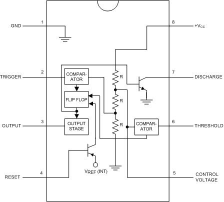
5 Pin Configuration and Functions
D, P, and DGK Packages
8-Pin SOIC, PDIP, and VSSOP
Top View

Pin Functions
| PIN | I/O | DESCRIPTION | |
|---|---|---|---|
| NO. | NAME | ||
| 5 | Control Voltage | I | Controls the threshold and trigger levels. It determines the pulse width of the output waveform. An external voltage applied to this pin can also be used to modulate the output waveform |
| 7 | Discharge | I | Open collector output which discharges a capacitor between intervals (in phase with output). It toggles the output from high to low when voltage reaches 2/3 of the supply voltage |
| 1 | GND | O | Ground reference voltage |
| 3 | Output | O | Output driven waveform |
| 4 | Reset | I | Negative pulse applied to this pin to disable or reset the timer. When not used for reset purposes, it should be connected to VCC to avoid false triggering |
| 6 | Threshold | I | Compares the voltage applied to the terminal with a reference voltage of 2/3 Vcc. The amplitude of voltage applied to this terminal is responsible for the set state of the flip-flop |
| 2 | Trigger | I | Responsible for transition of the flip-flop from set to reset. The output of the timer depends on the amplitude of the external trigger pulse applied to this pin. |
| 8 | V+ | I | Supply voltage with respect to GND |