SNOSB23F October   2008  – July 2019 LM5575-Q1

PRODUCTION DATA.  

  1. Features
  2. Applications
  3. Description
    1.     Device Images
      1.      Simplified Schematic
  4. Revision History
  5. Pin Configuration and Functions
    1.     Pin Functions
  6. Specifications
    1. 6.1 Absolute Maximum Ratings
    2. 6.2 ESD Ratings
    3. 6.3 Recommended Operating Conditions
    4. 6.4 Thermal Information
    5. 6.5 Electrical Characteristics
    6. 6.6 Typical Characteristics
  7. Detailed Description
    1. 7.1 Overview
    2. 7.2 Functional Block Diagram
    3. 7.3 Feature Description
      1. 7.3.1 Shutdown and Standby
      2. 7.3.2 Current Limit
      3. 7.3.3 Soft Start
      4. 7.3.4 Thermal Protection
    4. 7.4 Device Functional Modes
      1. 7.4.1 High-Voltage Start-Up Regulator
      2. 7.4.2 Oscillator and Sync Capability
      3. 7.4.3 Error Amplifier and PWM Comparator
      4. 7.4.4 Ramp Generator
      5. 7.4.5 BOOST Pin
      6. 7.4.6 Maximum Duty Cycle and Input Dropout Voltage
  8. Application and Implementation
    1. 8.1 Application Information
      1. 8.1.1 Bias Power Dissipation Reduction
    2. 8.2 Typical Application
      1. 8.2.1 Design Requirements
      2. 8.2.2 Detailed Design Procedure
        1. 8.2.2.1  Custom Design With WEBENCH® Tools
        2. 8.2.2.2  External Components
        3. 8.2.2.3  R3 (RT)
        4. 8.2.2.4  L1
        5. 8.2.2.5  C3 (CRAMP)
        6. 8.2.2.6  C9, C10
        7. 8.2.2.7  D1
        8. 8.2.2.8  C1, C2
        9. 8.2.2.9  C8
        10. 8.2.2.10 C7
        11. 8.2.2.11 C4
        12. 8.2.2.12 R5, R6
        13. 8.2.2.13 R1, R2, C12
        14. 8.2.2.14 R7, C11
        15. 8.2.2.15 R4, C5, C6
      3. 8.2.3 Application Curves
  9. Power Supply Recommendations
  10. 10Layout
    1. 10.1 Layout Guidelines
    2. 10.2 Layout Examples
    3. 10.3 Thermal Considerations
  11. 11Device and Documentation Support
    1. 11.1 Device Support
      1. 11.1.1 Custom Design With WEBENCH® Tools
    2. 11.2 Receiving Notification of Documentation Updates
    3. 11.3 Community Resources
    4. 11.4 Trademarks
    5. 11.5 Electrostatic Discharge Caution
    6. 11.6 Glossary
  12. 12Mechanical, Packaging, and Orderable Information

Package Options

Mechanical Data (Package|Pins)
Thermal pad, mechanical data (Package|Pins)
Orderable Information

Bias Power Dissipation Reduction

Buck regulators operating with high input voltage can dissipate an appreciable amount of power for the bias of the IC. The VCC regulator must step down the input voltage VIN to a nominal VCC level of 7 V. The large voltage drop across the VCC regulator translates into a large power dissipation within the VCC regulator. There are several techniques that can significantly reduce this bias regulator power dissipation. Figure 14 and Figure 15 depict two methods to bias the IC from the output voltage. In each case, the internal VCC regulator is used to initially bias the VCC pin. After the output voltage is established, the VCC pin potential is raised higher than the nominal 7-V regulation level, which effectively disables the internal VCC regulator. The voltage applied to the VCC pin should never exceed 14 V. The VCC voltage should never be larger than the VIN voltage.
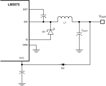
LM5575-Q1 30070818.gifFigure 14. VCC Bias From VOUT for 8 V < VOUT < 14 V
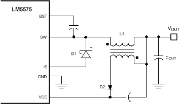
LM5575-Q1 30070819.gifFigure 15. VCC Bias With Additional Winding on the Output Inductor