SNVS447J January 2007 – November 2014 LM5576 , LM5576-Q1
PRODUCTION DATA.
- 1 Features
- 2 Applications
- 3 Description
- 4 Revision History
- 5 Pin Configuration and Functions
- 6 Specifications
- 7 Detailed Description
- 8 Application and Implementation
- 9 Power Supply Recommendations
- 10Layout
- 11Device and Documentation Support
- 12Mechanical, Packaging, and Orderable Information
Package Options
Mechanical Data (Package|Pins)
- PWP|20
Thermal pad, mechanical data (Package|Pins)
- PWP|20
Orderable Information
7 Detailed Description
7.1 Overview
The LM5576 switching regulator features all of the functions necessary to implement an efficient high voltage buck regulator using a minimum of external components. This easy to use regulator integrates a 75 V N-Channel buck switch with an output current capability of 3 Amps. The regulator control method is based on current mode control utilizing an emulated current ramp. Peak current mode control provides inherent line voltage feed-forward, cycle-by-cycle current limiting, and ease of loop compensation. The use of an emulated control ramp reduces noise sensitivity of the pulse-width modulation circuit, allowing reliable processing of very small duty cycles necessary in high input voltage applications. The operating frequency is user programmable from 50 kHz to 500 kHz. An oscillator synchronization pin allows multiple LM5576 regulators to self synchronize or be synchronized to an external clock. The output voltage can be set as low as 1.225 V. Fault protection features include, current limiting, thermal shutdown and remote shutdown capability. The device is available in the HTSSOP-20 package featuring an exposed pad to aid thermal dissipation.
The functional block diagram and typical application of the LM5576 are shown in the Functional Block Diagram section. The LM5576 can be applied in numerous applications to efficiently step-down a high, unregulated input voltage. The device is well suited for telecom, industrial and automotive power bus voltage ranges.
7.2 Functional Block Diagram

7.3 Feature Description
7.3.1 Shutdown / Standby
The LM5576 contains a dual level Shutdown (SD) circuit. When the SD pin voltage is below 0.7 V, the regulator is in a low current shutdown mode. When the SD pin voltage is greater than 0.7 V but less than 1.225 V, the regulator is in standby mode. In standby mode the VCC regulator is active but the output switch is disabled. When the SD pin voltage exceeds 1.225 V, the output switch is enabled and normal operation begins. An internal 5 µA pull-up current source configures the regulator to be fully operational if the SD pin is left open.
An external set-point voltage divider from VIN to GND can be used to set the operational input range of the regulator. The divider must be designed such that the voltage at the SD pin will be greater than 1.225 V when VIN is in the desired operating range. The internal 5 µA pull-up current source must be included in calculations of the external set-point divider. Hysteresis of 0.1 V is included for both the shutdown and standby thresholds. The SD pin is internally clamped with a 1 kΩ resistor and an 8 V zener clamp. The voltage at the SD pin should never exceed 14 V. If the voltage at the SD pin exceeds 8 V, the bias current will increase at a rate of 1 mA/V.
The SD pin can also be used to implement various remote enable / disable functions. Pulling the SD pin below the 0.7 V threshold totally disables the controller. If the SD pin voltage is above 1.225 V the regulator will be operational.
7.3.2 Soft-Start
The soft-start feature allows the regulator to gradually reach the initial steady state operating point, thus reducing start-up stresses and surges. The internal soft-start current source, set to 10 µA, gradually increases the voltage of an external soft-start capacitor connected to the SS pin. The soft-start capacitor voltage is connected to the reference input of the error amplifier. Various sequencing and tracking schemes can be implemented using external circuits that limit or clamp the voltage level of the SS pin.
In the event a fault is detected (over-temperature, VCC UVLO, SD) the soft-start capacitor will be discharged. When the fault condition is no longer present a new soft-start sequence will commence.
7.3.3 Thermal Protection
Internal Thermal Shutdown circuitry is provided to protect the integrated circuit in the event the maximum junction temperature is exceeded. When activated, typically at 165°C (Q1 version) and 180°C (Q0 version), the controller is forced into a low power reset state, disabling the output driver and the bias regulator. This feature is provided to prevent catastrophic failures from accidental device overheating.
7.4 Device Functional Modes
7.4.1 High Voltage Start-Up Regulator
The LM5576 contains a dual-mode internal high voltage startup regulator that provides the CC bias supply for the PWM controller and boot-strap MOSFET gate driver. The input pin (VIN) can be connected directly to the input voltage, as high as 75 Volts. For input voltages below 9 V, a low dropout switch connects VCC directly to VIN. In this supply range, VCC is approximately equal to VIN. For VIN voltage greater than 9 V, the low dropout switch is disabled and the VCC regulator is enabled to maintain VCC at approximately 7 V. The wide operating range of 6 V to 75 V is achieved through the use of this dual mode regulator.
The output of the VCC regulator is current limited to 25 mA. Upon power up, the regulator sources current into the capacitor connected to the VCC pin. When the voltage at the VCC pin exceeds the VCC UVLO threshold of 5.35 V and the SD pin is greater than 1.225 V, the output switch is enabled and a soft-start sequence begins. The output switch remains enabled until VCC falls below 5.0 V or the SD pin falls below 1.125 V.
An auxiliary supply voltage can be applied to the VCC pin to reduce the IC power dissipation. If the auxiliary voltage is greater than 7.3 V, the internal regulator will essentially shut off, reducing the IC power dissipation. The VCC regulator series pass transistor includes a diode between VCC and VIN that should not be forward biased in normal operation. Therefore the auxiliary VCC voltage should never exceed the VIN voltage.
In high voltage applications extra care should be taken to ensure the VIN pin does not exceed the absolute maximum voltage rating of 76 V. During line or load transients, voltage ringing on the VIN line that exceeds the Absolute Maximum Ratings can damage the IC. Both careful PC board layout and the use of quality bypass capacitors located close to the VIN and GND pins are essential.
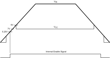 Figure 10. VIN and VCC Sequencing
7.4.2 Oscillator and Sync Capability
The LM5576 oscillator frequency is set by a single external resistor connected between the RT pin and the AGND pin. The RT resistor should be located very close to the device and connected directly to the pins of the IC (RT and AGND).To set a desired oscillator frequency (F), the necessary value for the RT resistor can be calculated from the following equation:

The SYNC pin can be used to synchronize the internal oscillator to an external clock. The external clock must be of higher frequency than the free-running frequency set by the RT resistor. A clock circuit with an open drain output is the recommended interface from the external clock to the SYNC pin. The clock pulse duration should be greater than 15 ns.
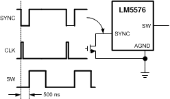 Figure 11. Sync From External Clock
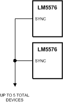 Figure 12. Sync From Multiple Devices
Multiple LM5576 devices can be synchronized together simply by connecting the SYNC pins together. In this configuration all of the devices will be synchronized to the highest frequency device. The diagram in Figure 13 illustrates the SYNC input/output features of the LM5576. The internal oscillator circuit drives the SYNC pin with a strong pull-down / weak pull-up inverter. When the SYNC pin is pulled low either by the internal oscillator or an external clock, the ramp cycle of the oscillator is terminated and a new oscillator cycle begins. Thus, if the SYNC pins of several LM5576 ICs are connected together, the IC with the highest internal clock frequency will pull the connected SYNC pins low first and terminate the oscillator ramp cycles of the other ICs. The LM5576 with the highest programmed clock frequency will serve as the master and control the switching frequency of the all the devices with lower oscillator frequency.
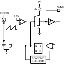 Figure 13. Simplified Oscillator Block Diagram and Sync I/O Circuit
7.4.3 Error Amplifier and PWM Comparator
The internal high gain error amplifier generates an error signal proportional to the difference between the regulated output voltage and an internal precision reference (1.225 V). The output of the error amplifier is connected to the COMP pin allowing the user to provide loop compensation components, generally a type II network, as illustrated in the Functional Block Diagram section. This network creates a pole at DC, a zero and a noise reducing high frequency pole. The PWM comparator compares the emulated current sense signal from the RAMP generator to the error amplifier output voltage at the COMP pin.
7.4.4 Ramp Generator
The ramp signal used in the pulse width modulator for current mode control is typically derived directly from the buck switch current. This switch current corresponds to the positive slope portion of the output inductor current. Using this signal for the PWM ramp simplifies the control loop transfer function to a single pole response and provides inherent input voltage feed-forward compensation. The disadvantage of using the buck switch current signal for PWM control is the large leading edge spike due to circuit parasitics that must be filtered or blanked. Also, the current measurement may introduce significant propagation delays. The filtering, blanking time and propagation delay limit the minimum achievable pulsewidth. In applications where the input voltage may be relatively large in comparison to the output voltage, controlling small pulsewidths and duty cycles is necessary for regulation. The LM5576 utilizes a unique ramp generator, which does not actually measure the buck switch current but rather reconstructs the signal. Reconstructing or emulating the inductor current provides a ramp signal to the PWM comparator that is free of leading edge spikes and measurement or filtering delays. The current reconstruction is comprised of two elements; a sample & hold DC level and an emulated current ramp.
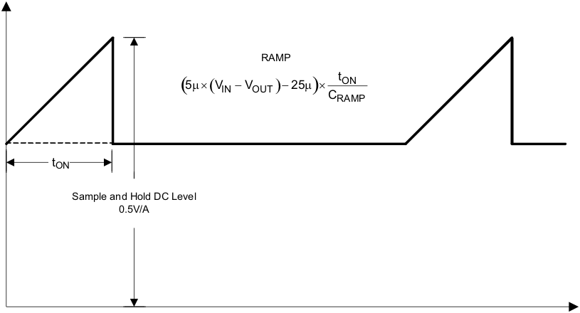 Figure 14. Composition of Current Sense Signal
The sample & hold DC level illustrated in Figure 14 is derived from a measurement of the re-circulating Schottky diode anode current. The re-circulating diode anode should be connected to the IS pin. The diode current flows through an internal current sense resistor between the IS and PGND pins. The voltage level across the sense resistor is sampled and held just prior to the onset of the next conduction interval of the buck switch. The diode current sensing and sample & hold provide the DC level of the reconstructed current signal. The positive slope inductor current ramp is emulated by an external capacitor connected from the RAMP pin to AGND and an internal voltage controlled current source. The ramp current source that emulates the inductor current is a function of the VIN and VOUT voltages per Equation 2:
Proper selection of the RAMP capacitor depends upon the selected value of the output inductor. The value of CRAMP can be selected from:
where
- L is the value of the output inductor in Henrys
With this value, the scale factor of the emulated current ramp will be approximately equal to the scale factor of the DC level sample and hold ( 0.5 V / A). The CRAMP capacitor should be located very close to the device and connected directly to the pins of the IC (RAMP and AGND).
For duty cycles greater than 50%, peak current mode control circuits are subject to sub-harmonic oscillation. Sub-harmonic oscillation is normally characterized by observing alternating wide and narrow pulses at the switch node. Adding a fixed slope voltage ramp (slope compensation) to the current sense signal prevents this oscillation. The 25 µA of offset current provided from the emulated current source adds some fixed slope to the ramp signal. In some high output voltage, high duty cycle applications, additional slope may be required. In these applications, a pull-up resistor may be added between the VCC and RAMP pins to increase the ramp slope compensation.
For VOUT > 7.5 V:
Calculate optimal slope current, IOS = VOUT x 5 µA/V.
For example, at VOUT = 10 V, IOS = 50 µA.
Install a resistor from the RAMP pin to VCC:
 Figure 15. RRAMP to VCC for VOUT > 7.5 V
Note that the emulated ramp signal on CRAMP is applied to the current limit comparator as described in the Current Limit section below. Increasing the ramp slope will result in lower current limit threshold. This can lower the output current capability of the part to less than 3 A in some conditions. The resulting current limit threshold can be calculated by the following equation:

where
- VCL = 2.1 V
- gm = 5 µA/V
- Ioffset = 25 µA
- A x Rs = 0.5 V/A
- VCC = 7 V
- T = switching period
- D = duty cycle (approximately VOUT / VIN)
- L = inductor value
- CRAMP = ramp capacitor value
- RRAMP = ramp resistor value
If the recommended CRAMP and RRAMP values are used, then the following simplified equation calculates the current limit threshold:

7.4.5 Maximum Duty Cycle / Input Drop-Out Voltage
There is a forced off-time of 500 ns implemented each cycle to ensure sufficient time for the diode current to be sampled. This forced off-time limits the maximum duty cycle of the buck switch. The maximum duty cycle will vary with the operating frequency.
where
- Fs is the oscillator frequency
Limiting the maximum duty cycle will raise the input dropout voltage. The input dropout voltage is the lowest input voltage required to maintain regulation of the output voltage. An approximation of the input dropout voltage is:

where
- VD is the voltage drop across the re-circulatory diode
Operating at high switching frequency raises the minimum input voltage necessary to maintain regulation.
7.4.6 Boost Pin
The LM5576 integrates an N-Channel buck switch and associated floating high voltage level shift / gate driver. This gate driver circuit works in conjunction with an internal diode and an external bootstrap capacitor. A 0.022 µF ceramic capacitor, connected with short traces between the BST pin and SW pin, is recommended. During the off-time of the buck switch, the SW pin voltage is approximately -0.5 V and the bootstrap capacitor is charged from VCC through the internal bootstrap diode. When operating with a high PWM duty cycle, the buck switch will be forced off each cycle for 500 ns to ensure that the bootstrap capacitor is recharged.
Under very light load conditions or when the output voltage is pre-charged, the SW voltage will not remain low during the off-time of the buck switch. If the inductor current falls to zero and the SW pin rises, the bootstrap capacitor will not receive sufficient voltage to operate the buck switch gate driver. For these applications, the PRE pin can be connected to the SW pin to pre-charge the bootstrap capacitor. The internal pre-charge MOSFET and diode connected between the PRE pin and PGND turns on each cycle for 265 ns just prior to the onset of a new switching cycle. If the SW pin is at a normal negative voltage level (continuous conduction mode), then no current will flow through the pre-charge MOSFET/diode. For output voltages above 5 V, a minimum load current may still be required to ensure that the SW voltage is pulled low enough to recharge the bootstrap capacitor.
7.4.7 Current Limit
The LM5576 contains a unique current monitoring scheme for control and over-current protection. When set correctly, the emulated current sense signal provides a signal which is proportional to the buck switch current with a scale factor of 0.5 V / A. The emulated ramp signal is applied to the current limit comparator. If the emulated ramp signal exceeds 2.1 V (4.2 A) the present current cycle is terminated (cycle-by-cycle current limiting). In applications with small output inductance and high input voltage the switch current may overshoot due to the propagation delay of the current limit comparator. If an overshoot should occur, the diode current sampling circuit will detect the excess inductor current during the off-time of the buck switch. If the sample & hold DC level exceeds the 2.1 V current limit threshold, the buck switch will be disabled and skip pulses until the diode current sampling circuit detects the inductor current has decayed below the current limit threshold. This approach prevents current runaway conditions due to propagation delays or inductor saturation since the inductor current is forced to decay following any current overshoot.