-
LM57-Q1 Resistor-Programmable Temperature Switch and Analog Temperature Sensor
- 1 Features
- 2 Applications
- 3 Description
- 4 Device Comparison Table
- 5 Pin Configuration and Functions
- 6 Specifications
-
7 Detailed Description
- 7.1 Overview
- 7.2 Functional Block Diagram
- 7.3 Feature Description
- 7.4 Device Functional Modes
- 8 Application and Implementation
- 9 Power Supply Recommendations
- 10Layout
- 11Device and Documentation Support
- 12Mechanical, Packaging, and Orderable Information
- IMPORTANT NOTICE
Package Options
Mechanical Data (Package|Pins)
- PW|8
Thermal pad, mechanical data (Package|Pins)
Orderable Information
LM57-Q1 Resistor-Programmable Temperature Switch and Analog Temperature Sensor
1 Features
- Qualified for Automotive Applications, for Commercial Device See LM57 Data Sheet
- AEC-Q100 Qualified with the Following Results:
- Temperature Grade 0 Extended: −50°C to +160°C with Excursions up to 170°C Operating Temperature Range
- Temperature Grade 0: −50°C to +150°C Operating Temperature Range
- Temperature Grade 1: −50°C to +125°C Operating Temperature Range
- HBM ESD Component Classification Level 2
- CDM ESD Component Classification Level C5
- Trip Temperature Set by External Resistors with
Accuracy of ±2.3°C from −40°C to +150°C - Resistor Tolerance Contributes Zero Error
- Push-Pull and Open-Drain Switch Outputs
- Wide Operating Temperature Range of −50°C to 160°C
- Very Linear Analog VTEMP Temp Sensor Output
with ±1.3°C Accuracy from −50°C to +150°C - Short-Circuit Protected Analog and Digital Outputs
- Latching Function for Digital Outputs
- TRIP-TEST Pin Allows In-System Testing
- Low Power Minimizes Self-Heating to Under 0.02°C
2 Applications
- Automotive
- Down Hole and Avionics
3 Description
The LM57-Q1 device is a precision, dual-output, temperature switch with analog temperature sensor output for wide temperature applications such as automotive grade. The trip temperature (TTRIP) is selected from 256 possible values in the range of –40°C to 160°C. The VTEMP is a class AB analog voltage output that is proportional to temperature with a programmable negative temperature coefficient (NTC). Two external 1% resistors set the TTRIP and VTEMP slope. The digital and analog outputs enable protection and monitoring of system thermal events.
Built-in thermal hysteresis (THYST) prevents the digital outputs from oscillating. The TOVER and TOVER digital outputs will assert when the die temperature exceeds TTRIP and will de-assert when the temperature falls below a temperature equal to TTRIP minus THYST.
TOVER is active-high with a push-pull structure. TOVER is active-low with an open-drain structure. Tying TOVER to TRIP-TEST will latch the output after it trips. The output can be cleared by forcing TRIP-TEST low. Driving the TRIP-TEST high will assert the digital outputs. A processor can check the state of TOVER or TOVER, confirming they changed to an active state. This allows for in situ verification that the comparator and output circuitry are functional after system assembly. When TRIP-TEST is high, the trip-level reference voltage appears at the VTEMP pin. The system could then use this voltage to calculate the threshold of the LM57-Q1.
- For all available packages, see the orderable addendum at the end of the data sheet.
- For device comparison see Device Comparison Table.
LM57-Q1 Overtemperature Alarm

Temperature Transfer Function

4 Device Comparison Table
| ORDER NUMBER | PACKAGE | GRADE (TEMP RANGE) | VTEMP ACCURACY | TRIP POINT ACCURACY | HYSTERESIS |
|---|---|---|---|---|---|
| LM57BISD-5, LM57BISDX-5(1) | WSON/SD/NGR/DFN (8) | Commercial (-50°C to 150°C) | ±0.8°C | ±1.5°C | 5°C |
| LM57BISD-10, LM57BISDX-10(1) | WSON/SD/NGR/DFN (8) | Commercial (-50°C to 150°C) | ±0.8°C | ±1.5°C | 10°C |
| LM57CISD-5, LM57CISD-5(1) | WSON/SD/NGR/DFN (8) | Commercial (-50°C to 150°C) | ±1.3°C | ±2.3°C | 5°C |
| LM57CISD-10, LM57CISDX-10(1) | WSON/SD/NGR/DFN (8) | Commercial (-50°C to 150°C) | ±1.3°C | ±2.3°C | 10°C |
| LM57FPW, LM57FPWR(1) | PW/TSSOP (8) | Commercial (-50°C to 150°C) | ±1.3°C | ±2.3°C | 5°C |
| LM57TPW, LM57TPWR(1) | PW/TSSOP (8) | Commercial (-50°C to 150°C) | ±1.3°C | ±2.3°C | 10°C |
| LM57FSPWQ1, LM57FSPWRQ1 | PW/TSSOP (8) | Automotive Grade 0 Extended (-50°C to 160°C) | ±1.3°C | ±2.3°C | 5°C |
| LM57TSPWQ1, LM57TSPWRQ1 | PW/TSSOP (8) | Automotive Grade 0 Extended (-50°C to 160°C) | ±1.3°C | ±2.3°C | 10°C |
| LM57FEPWQ1, LM57FEPWRQ1 | PW/TSSOP (8) | Automotive Grade 0 Standard (-50°C to 150°C) | ±1.3°C | ±2.3°C | 5°C |
| LM57TEPWQ1, LM57TEPWRQ1 | PW/TSSOP (8) | Automotive Grade 0 Standard (-50°C to 150°C) | ±1.3°C | ±2.3°C | 10°C |
| LM57FQPWQ1, LM57FQPWRQ1 | PW/TSSOP (8) | Automotive Grade 1 Standard (-50°C to 125°C) | ±1.3°C | ±2.3°C | 5°C |
| LM57TQPWQ1, LM57TQPWRQ1 | PW/TSSOP (8) | Automotive Grade 1 Standard (-50°C to 125°C) | ±1.3°C | ±2.3°C | 10°C |
5 Pin Configuration and Functions

Pin Functions
| PIN | TYPE | EQUIVALENT CIRCUIT | DESCRIPTION | |
|---|---|---|---|---|
| NAME | NO. | |||
| GND | 1 | Ground | — | Power supply ground |
| SENSE1 | 2 | — | 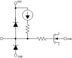 |
Trip-point resistor sense. One of two sense pins which selects the temperature at which TOVER and TOVER will assert. |
| SENSE2 | 3 | — |  |
Trip-point resistor sense. One of two sense pins which selects the temperature at which TOVER and TOVER will assert. |
| VDD | 4 | Power | Supply voltage | |
| TRIP TEST |
5 | Digital Input |  |
TRIP TEST pin. Active High input. If TRIP TEST = 0 (default), then the VTEMP output has the analog temperature sensor output voltage. If TRIP TEST = 1, then TOVER and TOVER outputs are asserted and VTEMP = VTRIP, the temperature trip voltage. Tie this pin to ground if not used. |
| TOVER | 6 | Digital Output |  |
Overtemperature switch output Active low, open-drain (see LM57-Q1 VTEMP Voltage-to-Temperature Equations regarding required pullup resistor.) Asserted when the measured temperature exceeds the Trip Point Temperature or if TRIP TEST = 1 This pin may be left open if not used. |
| TOVER | 7 | Digital Output |  |
Overtemperature switch output Active high, push-pull Asserted when the measured temperature exceeds the trip point temperature or if TRIP TEST = 1 This pin may be left open if not used. |
| VTEMP | 8 | Analog Output |  |
VTEMP analog voltage output If TRIP TEST = 0, then VTEMP = VTS, temperature sensor output voltage If TRIP TEST = 1, then VTEMP = VTRIP, temperature trip voltage This pin may be left open if not used. |
6 Specifications
6.1 Absolute Maximum Ratings
over operating free-air temperature range (unless otherwise noted) (1)(2)| MIN | MAX | UNIT | ||
|---|---|---|---|---|
| Supply voltage | −0.3 | 6 | V | |
| Voltage at TOVER | −0.3 | 6 | V | |
| Voltage at TOVER , VTEMP, TRIP-TEST, SENSE1, and SENSE2 | −0.3 | (VDD + 0.3 V) | V | |
| Current at any pin | 5 | mA | ||
| Storage temperature for LM57FSPWQ1 and LM57TSPWQ1 | −65 | 175 | °C | |
| Storage temperature for all LM57-Q1 except LM57FSPWQ1 and LM57TSPWQ1 | −65 | 150 | °C | |
6.2 ESD Ratings
| VALUE | UNIT | |||
|---|---|---|---|---|
| V(ESD) | Electrostatic discharge | Human-body model (HBM), per AEC Q100-002 (1) | ±2000 | V |
| Charged-device model (CDM), per AEC Q100-011 | ±750 | |||
6.3 Recommended Operating Conditions
| MIN | NOM | MAX | UNIT | ||
|---|---|---|---|---|---|
| FOR ALL PARTS GRADE 0 AND GRADE 1 EXCEPT GRADE 0 EXTENDED (LM57FSPWQ1 and LM57TSPWQ1) | |||||
| Supply voltage | 2.4 | 5.5 | V | ||
| Free air temperature range (TMIN ≤ TA ≤ TMAX) | LM57FEPWQ1, and LM57TEPWQ1 | −50 | 150 | °C | |
| LM57FQPWQ1, LM57TQPWQ1 | -50 | 125 | °C | ||
| GRADE 0 EXTENDED (LM57FSPWQ1 AND LM57TSPWQ1) | |||||
| Supply voltage | 2.4 | 5.5 | V | ||
| Free air temperature range (TMIN ≤ TA ≤ TMAX) | Temperature Profile for LM57-Q1 Automotive Grade 0 Extended High Temperature Operational Life Test (HTOL) - Hours of Operation: (1) | −50 | 170 | °C | |
| 1700 hours at TJ = TC = 160°C | |||||
| 10 hours at TJ = TC = 170°C | |||||
6.4 Thermal Information
| THERMAL METRIC (1) | LM57-Q1 | UNIT | |
|---|---|---|---|
| PW (TSSOP) | |||
| 8 PINS | |||
| RθJA | Junction-to-ambient thermal resistance | 183 | °C/W |
| RθJC(top) | Junction-to-case (top) thermal resistance | 66 | °C/W |
| RθJB | Junction-to-board thermal resistance | 111 | °C/W |
| ψJT | Junction-to-top characterization parameter | 8 | °C/W |
| ψJB | Junction-to-board characterization parameter | 110 | °C/W |
| RθJC(bot) | Junction-to-case (bottom) thermal resistance | — | °C/W |
6.5 Electrical Characteristics
Unless otherwise noted, these specifications apply for VDD = 2.4 to 5.5 V and over free air temperature range. These limits do not include DC load regulation. These stated accuracy limits are with reference to the values in Table 1.| PARAMETER | TEST CONDITIONS | MIN | TYP | MAX | UNIT | |||
|---|---|---|---|---|---|---|---|---|
| TRIP POINT ACCURACY FOR ALL LM57-Q1 EXCEPT LM57FSPWQ1 AND LM57TSPWQ1 | ||||||||
| Trip Point Accuracy (Includes 1% set-resistor tolerance) |
J2 | TA = −41°C to 52°C | VDD = 2.4 V to 5.5 V | ±2.3 | °C | |||
| J3 | TA = 52°C to 97°C | VDD = 2.4 V to 5.5 V | ±2.3 | °C | ||||
| J4 | TA = 97°C to 119°C | VDD = 2.4 V to 5.5 V | ±2.3 | °C | ||||
| J5 | TA = 119°C to free air temperature max | VDD = 2.4 V to 5.5 V | ±2.3 | °C | ||||
| TRIP POINT ACCURACY FOR LM57-Q1 AUTOMOTIVE GRADE 0 EXTENDED (LM57FSPWQ1 and LM57TSPWQ1) | ||||||||
| Trip point accuracy (Includes 1% set-resistor tolerance) |
J2 | TA = −41°C to 52°C | VDD = 2.4 V to 5.5 V | ±2.3 | °C | |||
| J3 | TA = 52°C to 97°C | |||||||
| J4 | TA = 97°C to 119°C | |||||||
| J5 | TA = 119°C to 160°C | |||||||
| J5 | TA = 150°C to 160°C | VDD = 2.4 V to 5.5 V | ±2.5 | |||||
| VTEMP ANALOG TEMPERATURE SENSOR OUTPUT ACCURACY FOR ALL LM57-Q1 EXCEPT LM57FSPWQ1 and LM57TSPWQ1 | ||||||||
| VTEMP Accuracy (These stated accuracy limits are with reference to the values in Table 1, LM57-Q1 VTEMP Temperature-to-Voltage.) |
J2 | TA = −50°C to free air temperature max | VDD = 2.4 V to 5.5 V | ±1.3 | °C | |||
| J3 | TA = −50°C to free air temperature max | VDD = 2.4 V to 5.5 V | ±1.3 | °C | ||||
| J4 | TA = 20°C to 50°C | VDD = 2.4 V to 5.5 V | ±1.3 | °C | ||||
| TA = 0°C to free air temperature max | VDD = 2.7 V to 5.5 V | ±1.3 | ||||||
| TA = −50°C to 0°C | VDD = 3.1 V to 5.5 V | ±1.3 | ||||||
| J5 | TA = 60°C to free air temperature max | VDD = 2.4 V to 5.5 V | ±1.3 | °C | ||||
| TA = 20°C to 50°C | VDD = 2.9 V to 5.5 V | ±1.3 | ||||||
| TA = 0°C to free air temperature max | VDD = 3.2 V to 5.5 V | ±1.3 | ||||||
| TA = −50°C to 0°C | VDD = 4 V to 5.5 V | ±1.3 | ||||||
| VTEMP ANALOG TEMPERATURE SENSOR OUTPUT ACCURACY FOR LM57-Q1 AUTOMOTIVE GRADE 0 EXTENDED (LM57FSPWQ1 and LM57TSPWQ1) | ||||||||
| VTEMP accuracy (These stated accuracy limits are with reference to the values in Table 1, LM57-Q1 VTEMP temperature-to-voltage.) |
J2 | TA = 150°C to 160°C | VDD = 2.4 V to 5.5 V | ±1.5 | °C | |||
| TA = –50°C to 150°C | ±1.3 | |||||||
| J3 | TA = 150°C to 160°C | VDD = 2.4 V to 5.5 V | ±1.5 | °C | ||||
| TA = –50°C to 150°C | ±1.3 | |||||||
| J4 | TA = 20°C to 50°C | VDD = 2.4 V to 5.5 V | ±1.3 | °C | ||||
| TA = 0°C to 150°C | VDD = 2.7 V to 5.5 V | ±1.3 | ||||||
| TA = 150°C to 160°C | ±1.5 | |||||||
| TA = –50°C to 0°C | VDD = 3.1 V to 5.5 V | ±1.3 | ||||||
| J5 | TA = 150°C to 160°C | VDD = 2.4 V to 5.5 V | ±1.5 | °C | ||||
| TA = 60°C to 150°C | ±1.3 | |||||||
| TA = 20°C to 50°C | VDD = 2.9 V to 5.5 V | ±1.3 | ||||||
| TA = 0°C to 150°C | VDD = 3.2 V to 5.5 V | ±1.3 | ||||||
| TA = –50°C to 0°C | VDD = 4 V to 5.5 V | ±1.3 | ||||||
| OTHER TEMPERATURE SENSOR SPECIFICATIONS | ||||||||
| VTEMP sensor gain | J2: −50°C to 52°C | −5.166 | mV/°C | |||||
| J3: 52°C to 97°C | −7.752 | |||||||
| J4: 97°C to 119°C | −10.339 | |||||||
| J5: 119°C to 160°C | −12.924 | |||||||
| Line regulation DC: supply-to-VTEMP(1) | Temp = 90°C | 0.18 | mV | |||||
| 58 | μV/V | |||||||
| −84 | dB | |||||||
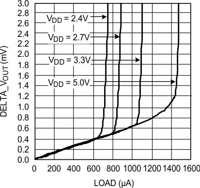
| Load regulation: VTEMP output (4) | Source ≤ 240 µA, (VDD – VTEMP) ≥ 200 mV; TA = −50°C to 150°C | −1 | mV | |||||
| Sink ≤ 300 µA, VTEMP ≥ 360 mV; TA = −50°C to 150°C | 1 | |||||||
| Source or sink = 100 µA; TA = −50°C to 150°C | 1 | Ω | ||||||
| Maximum Load capacitance: VTEMP output | No output series resistor required; (See VTEMP Capacitive Loads) | 1100 | pF | |||||
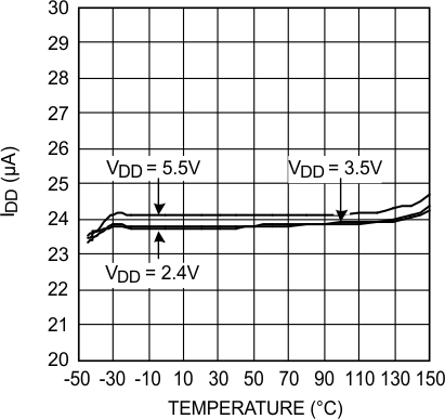
| IS | Supply current: quiescent (2) | for all LM57-Q1 for TA ≤ 150°C | 24 | 28 | µA | |||
| TA = 150°C to 160°C for LM57FSPWQ1 and LM57TSPWQ1 | 24 | 29 | µA | |||||
| TA = 170°C for LM57FSPWQ1 and LM57TSPWQ1 | 26 | µA | ||||||
| TRIP-TEST INPUT | ||||||||
| VIH | Logic 1 threshold voltage | VDD – 0.5 | V | |||||
| VIL | Logic 0 threshold voltage | 0.5 | V | |||||
| IIH | Logic 1 input current | 1.4 | 3 | µA | ||||
| IIL | Logic 0 input leakage current (3) | TA = −50°C to 150°C | 0.001 | 1 | µA | |||
| TOVER (PUSH-PULL, ACTIVE-HIGH) OUTPUT | ||||||||
| VOH | Logic 1 push-pull output voltage | Source ≤ 600 µA | VDD – 0.2 | V | ||||
| Source ≤ 1.2 mA | VDD – 0.45 | |||||||
| VOL | Logic 0 output voltage | Sink ≤ 600 µA | 0.2 | V | ||||
| Sink ≤ 1.2 mA | 0.45 | |||||||
| TOVER (OPEN-DRAIN, ACTIVE-LOW) OUTPUT | ||||||||
| VOL | Logic 0 output voltage | Sink ≤ 600 µA | 0.2 | V | ||||
| Sink ≤1.2 mA | 0.45 | |||||||
| IOH | Logic 1 output leakage current (3) | Temperature = 30°C; | 0.001 | 1 | µA | |||
| HYSTERESIS | ||||||||
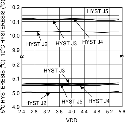
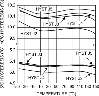
| THYST | Hysteresis temperature | 5°C hysteresis option (all LM57F for TA ≤ 150°C) | 4.7 | 5 | 5.4 | °C | ||
| 10°C hysteresis option (all LM57T for TA ≤ 150°C) | 9.6 | 10 | 10.6 | °C | ||||
| 5°C hysteresis option (LM57FSPWQ1); TA = 150°C to 160°C | 4.6 | 5 | 5.4 | °C | ||||
| 10°C hysteresis option (LM57TSPWQ1); TA = 150°C to 160°C | 9.4 | 10 | 10.6 | °C | ||||
6.6 Switching Characteristics
Unless otherwise noted, these specifications apply for VDD = 2.4 to 5.5 V over the free air temperature range.| PARAMETER | TEST CONDITIONS | MIN | TYP | MAX | UNIT | ||
|---|---|---|---|---|---|---|---|
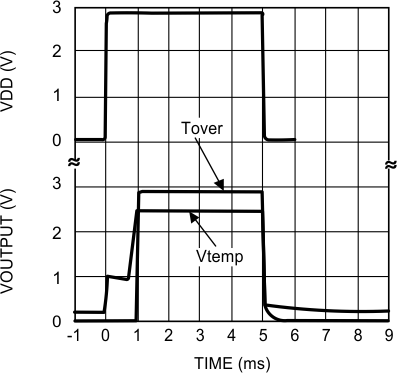
| tEN | Maximum time from power on to digital output enabled | 1.5 | ms | ||||
| tVTEMP | Maximum time from power on to analog temperature (VTEMP) valid | 1.5 | ms | ||||
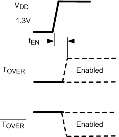 Figure 1. Definition of tEN
 Figure 2. Definition of tVTEMP
6.7 Typical Characteristics
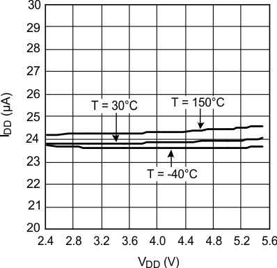
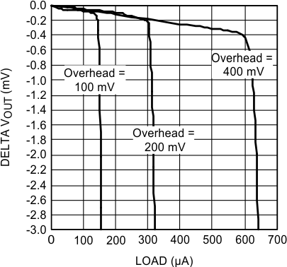
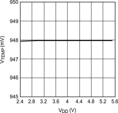
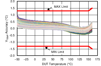
| Conditions: J2, VDD=5V |
