SNVSBM0B March   2020  – June 2021 LM61435-Q1

PRODUCTION DATA  

  1. Features
  2. Applications
  3. Description
  4. Revision History
  5. Device Comparison Table
  6. Pin Configuration and Functions
  7. Specifications
    1. 7.1 Absolute Maximum Ratings
    2. 7.2 ESD Ratings
    3. 7.3 Recommended Operating Conditions
    4. 7.4 Thermal Information
    5. 7.5 Electrical Characteristics
    6. 7.6 Timing Characteristics
    7. 7.7 Systems Characteristics
    8. 7.8 Typical Characteristics
  8. Detailed Description
    1. 8.1 Overview
    2. 8.2 Functional Block Diagram
    3. 8.3 Feature Description
      1. 8.3.1  EN/SYNC Uses for Enable and VIN UVLO
      2. 8.3.2  EN/SYNC Pin Uses for Synchronization
      3. 8.3.3  Clock Locking
      4. 8.3.4  Adjustable Switching Frequency
      5. 8.3.5  PGOOD Output Operation
      6. 8.3.6  Internal LDO, VCC UVLO, and BIAS Input
      7. 8.3.7  Bootstrap Voltage and VCBOOT-UVLO (CBOOT Pin)
      8. 8.3.8  Adjustable SW Node Slew Rate
      9. 8.3.9  Spread Spectrum
      10. 8.3.10 Soft Start and Recovery From Dropout
      11. 8.3.11 Output Voltage Setting
      12. 8.3.12 Overcurrent and Short Circuit Protection
      13. 8.3.13 Thermal Shutdown
      14. 8.3.14 Input Supply Current
    4. 8.4 Device Functional Modes
      1. 8.4.1 Shutdown Mode
      2. 8.4.2 Standby Mode
      3. 8.4.3 Active Mode
        1. 8.4.3.1 CCM Mode
        2. 8.4.3.2 Auto Mode - Light Load Operation
          1. 8.4.3.2.1 Diode Emulation
          2. 8.4.3.2.2 Frequency Reduction
        3. 8.4.3.3 FPWM Mode - Light Load Operation
        4. 8.4.3.4 Minimum On-time (High Input Voltage) Operation
        5. 8.4.3.5 Dropout
  9. Application and Implementation
    1. 9.1 Application Information
    2. 9.2 Typical Application
      1. 9.2.1 Design Requirements
      2. 9.2.2 Detailed Design Procedure
        1. 9.2.2.1  Choosing the Switching Frequency
        2. 9.2.2.2  Setting the Output Voltage
        3. 9.2.2.3  Inductor Selection
        4. 9.2.2.4  Output Capacitor Selection
        5. 9.2.2.5  Input Capacitor Selection
        6. 9.2.2.6  BOOT Capacitor
        7. 9.2.2.7  BOOT Resistor
        8. 9.2.2.8  VCC
        9. 9.2.2.9  BIAS
        10. 9.2.2.10 CFF and RFF Selection
        11. 9.2.2.11 External UVLO
      3. 9.2.3 Application Curves
  10. 10Power Supply Recommendations
  11. 11Layout
    1. 11.1 Layout Guidelines
      1. 11.1.1 Ground and Thermal Considerations
    2. 11.2 Layout Example
  12. 12Device and Documentation Support
    1. 12.1 Documentation Support
      1. 12.1.1 Related Documentation
    2. 12.2 Receiving Notification of Documentation Updates
    3. 12.3 Support Resources
    4. 12.4 Trademarks
    5. 12.5 Electrostatic Discharge Caution
    6. 12.6 Glossary
  13. 13Mechanical, Packaging, and Orderable Information

Package Options

Refer to the PDF data sheet for device specific package drawings

Mechanical Data (Package|Pins)
  • RJR|14
Thermal pad, mechanical data (Package|Pins)
Orderable Information
Diode Emulation

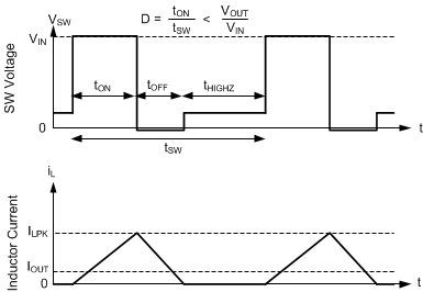
Diode emulation prevents reverse current through the inductor which requires a lower frequency needed to regulate given a fixed peak inductor current. Diode emulation also limits ripple current as frequency is reduced. With a fixed peak current, as output current is reduced to zero, frequency must be reduced to near zero to maintain regulation.
GUID-464583A7-C84D-430D-B6C9-E25E0B127108-low.gif
In auto mode, the low-side device is turned off once SW node current is near zero. As a result, once output current is less than half of what inductor ripple would be in CCM, the part operates in DCM which is equivalent to the statement that diode emulation is active.
Figure 8-15 PFM Operation

The LM61435-Q1 has a minimum peak inductor current setting while in auto mode. Once current is reduced to a low value with fixed input voltage, on-time is constant. Regulation is then achieved by adjusting frequency. This mode of operation is called PFM mode regulation.