SNVSBM0B March 2020 – June 2021 LM61435-Q1
PRODUCTION DATA
- 1 Features
- 2 Applications
- 3 Description
- 4 Revision History
- 5 Device Comparison Table
- 6 Pin Configuration and Functions
- 7 Specifications
-
8 Detailed Description
- 8.1 Overview
- 8.2 Functional Block Diagram
- 8.3
Feature Description
- 8.3.1 EN/SYNC Uses for Enable and VIN UVLO
- 8.3.2 EN/SYNC Pin Uses for Synchronization
- 8.3.3 Clock Locking
- 8.3.4 Adjustable Switching Frequency
- 8.3.5 PGOOD Output Operation
- 8.3.6 Internal LDO, VCC UVLO, and BIAS Input
- 8.3.7 Bootstrap Voltage and VCBOOT-UVLO (CBOOT Pin)
- 8.3.8 Adjustable SW Node Slew Rate
- 8.3.9 Spread Spectrum
- 8.3.10 Soft Start and Recovery From Dropout
- 8.3.11 Output Voltage Setting
- 8.3.12 Overcurrent and Short Circuit Protection
- 8.3.13 Thermal Shutdown
- 8.3.14 Input Supply Current
- 8.4 Device Functional Modes
- 9 Application and Implementation
- 10Power Supply Recommendations
- 11Layout
- 12Device and Documentation Support
- 13Mechanical, Packaging, and Orderable Information
Package Options
Refer to the PDF data sheet for device specific package drawings
Mechanical Data (Package|Pins)
- RJR|14
Thermal pad, mechanical data (Package|Pins)
Orderable Information
8.3.2 EN/SYNC Pin Uses for Synchronization
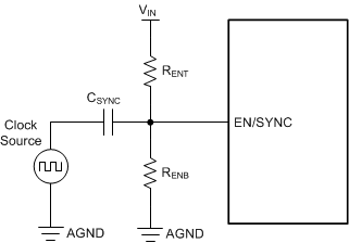
The LM61435-Q1 EN/SYNC pin can be used to synchronize the internal oscillator to an external clock. The internal oscillator can be synchronized by AC coupling a positive clock edge into the EN pin, as shown in Figure 8-2. It is recommended to keep the parallel combination value of RENT and RENB in the 100-kΩ range. RENT is required for synchronization, but RENB can be left unmounted. Switching action can be synchronized to an external clock ranging from 200 kHz to 2.2 MHz. The external clock must be off before start-up to allow proper start-up sequencing.
 Figure 8-2 Typical Implementation Allowing Synchronization Using the EN Pin
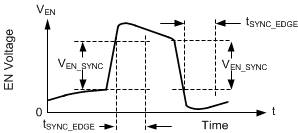
Referring to Figure 8-3, the AC-coupled voltage edge at the EN pin must exceed the SYNC amplitude threshold, VEN_SYNC_MIN, to trip the internal synchronization pulse detector. In addition, the minimum EN/SYNC rising pulse and falling pulse durations must be longer than tSYNC_EDGE(MIN) and shorter than the blanking time, tB. A 3.3-V or higher amplitude pulse signal coupled through a 1-nF capacitor, CSYNC, is suggested.
 Figure 8-3 Typical SYNC/EN Waveform
After a valid synchronization signal is applied for 2048 cycles, the clock frequency abruptly changes to that of the applied signal. Also, if the device in use has the spread-spectrum feature, the valid synchronization signal overrides spread spectrum, turning it off, and the clock switches to the applied clock frequency.