SNVSBD6C May 2019 – June 2021 LM61440
PRODUCTION DATA
- 1 Features
- 2 Applications
- 3 Description
- 4 Revision History
- 5 Device Comparison Table
- 6 Pin Configuration and Functions
- 7 Specifications
-
8 Detailed Description
- 8.1 Overview
- 8.2 Functional Block Diagram
- 8.3
Feature Description
- 8.3.1 EN/SYNC Uses for Enable and VIN UVLO
- 8.3.2 EN/SYNC Pin Uses for Synchronization
- 8.3.3 Clock Locking
- 8.3.4 Adjustable Switching Frequency
- 8.3.5 PGOOD Output Operation
- 8.3.6 Internal LDO, VCC UVLO, and BIAS Input
- 8.3.7 Bootstrap Voltage and VCBOOT-UVLO (CBOOT Pin)
- 8.3.8 Adjustable SW Node Slew Rate
- 8.3.9 Spread Spectrum
- 8.3.10 Soft Start and Recovery From Dropout
- 8.3.11 Output Voltage Setting
- 8.3.12 Overcurrent and Short Circuit Protection
- 8.3.13 Thermal Shutdown
- 8.3.14 Input Supply Current
- 8.4 Device Functional Modes
- 9 Application and Implementation
- 10Power Supply Recommendations
- 11Layout
- 12Device and Documentation Support
- 13Mechanical, Packaging, and Orderable Information
Package Options
Mechanical Data (Package|Pins)
- RJR|14
Thermal pad, mechanical data (Package|Pins)
Orderable Information
3 Description
The LM61440 is a high-performance, DC-DC synchronous step-down converter. With integrated high-side and low-side MOSFETs, up to 4 A of output current is delivered over a wide input range of 3.0 V to 36 V; tolerant of 42 V, easing input surge protection design. The LM61440 implements soft recovery from dropout eliminating overshoot on the output.
The LM61440 is specifically designed for minimal EMI. The device incorporates adjustable SW node rise time, low-EMI VQFN-HR package featuring low switch node ringing, and optimized pinout for ease of use. The switching frequency can be set or synchronized between 200 kHz and 2.2 MHz to avoid noise sensitive frequency bands. In addition the frequency can be selected for improved efficiency at low operating frequency or smaller solution size at high operating frequency.
Auto-mode enables frequency foldback when operating at light loads, allowing an unloaded current consumption of only 7 µA (typical) and high light load efficiency. Seamless transition between PWM and PFM modes, along with very low MOSFET ON resistances and an external bias input, ensures exceptional efficiency across the entire load range.
Electrical characteristics are specified over a junction temperature range of –40°C to +150°C. Find additional resources in the Related Documentation.
| PART NUMBER | PACKAGE(1) | BODY SIZE (NOM) |
|---|---|---|
| LM61440 | VQFN-HR (14) | 4.00 mm × 3.50 mm |
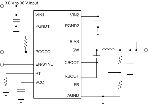
 Simplified Schematic
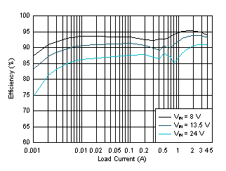
 Efficiency VOUT =
5 V, FSW = 2200 kHz