SNVSBD6C May 2019 – June 2021 LM61440
PRODUCTION DATA
- 1 Features
- 2 Applications
- 3 Description
- 4 Revision History
- 5 Device Comparison Table
- 6 Pin Configuration and Functions
- 7 Specifications
-
8 Detailed Description
- 8.1 Overview
- 8.2 Functional Block Diagram
- 8.3
Feature Description
- 8.3.1 EN/SYNC Uses for Enable and VIN UVLO
- 8.3.2 EN/SYNC Pin Uses for Synchronization
- 8.3.3 Clock Locking
- 8.3.4 Adjustable Switching Frequency
- 8.3.5 PGOOD Output Operation
- 8.3.6 Internal LDO, VCC UVLO, and BIAS Input
- 8.3.7 Bootstrap Voltage and VCBOOT-UVLO (CBOOT Pin)
- 8.3.8 Adjustable SW Node Slew Rate
- 8.3.9 Spread Spectrum
- 8.3.10 Soft Start and Recovery From Dropout
- 8.3.11 Output Voltage Setting
- 8.3.12 Overcurrent and Short Circuit Protection
- 8.3.13 Thermal Shutdown
- 8.3.14 Input Supply Current
- 8.4 Device Functional Modes
- 9 Application and Implementation
- 10Power Supply Recommendations
- 11Layout
- 12Device and Documentation Support
- 13Mechanical, Packaging, and Orderable Information
Package Options
Mechanical Data (Package|Pins)
- RJR|14
Thermal pad, mechanical data (Package|Pins)
Orderable Information
8.3.12 Overcurrent and Short Circuit Protection
The LM61440 is protected from overcurrent conditions with cycle-by-cycle current limiting on both the high-side and the low-side MOSFETs.
High-side MOSFET overcurrent protection is implemented by the nature of the peak-current mode control. The HS switch current is sensed when the HS is turned on after a short blanking time. Every switching cycle, the HS switch current is compared to either the minimum of a fixed current set point or the output of the voltage regulation loop minus slope compensation. Because the voltage loop has a maximum value and slope compensation increases with duty cycle, HS current limit decreases with increased duty cycle when duty cycle is above 35%.
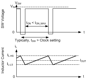
When the LS switch is turned on, the switch current is also sensed and monitored. Like the high-side device, the low-side device turns off as commanded by the voltage control loop and low-side current limit. If the LS switch current is higher than ILS_Limit at the end of a switching cycle, the switching cycle is extended until the LS current reduces below the limit. The LS switch is turned off once the LS current falls below its limit, and the HS switch is turned on again as long as at least one clock period has passed since the last time the HS device has turned on.
 Figure 8-12 Current Limit Waveforms
Since the current waveform assumes values between IL-HS and IL-LS, the maximum output current is very close to the average of these two values. Hysteretic control is used and current does not increase as output voltage approaches zero.
The LM61440 employs hiccup overcurrent protection if there is an extreme overload, and the following conditions are met for 128 consecutive switching cycles:
- Output voltage is below approximately 0.4 times the output voltage set point.
- Greater than tSS2 has passed since soft start has started; see Section 8.3.10.
- The part is not operating in dropout, which is defined as having minimum off-time controlled duty cycle.
In hiccup mode, the device shuts itself down and attempts to soft start after tW. Hiccup mode helps reduce the device power dissipation under severe overcurrent conditions and short circuits. See Figure 8-13.
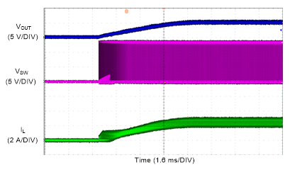
Once the overload is removed, the device recovers as though in soft start; see Figure 8-14.
 Figure 8-13 Inductor Current Bursts During Hiccup
 Figure 8-14 Short Circuit Recovery