SNVSBD5D May   2019  – July 2022 LM61460

PRODUCTION DATA  

  1. Features
  2. Applications
  3. Description
  4. Revision History
  5. Device Comparison Table
  6. Pin Configuration and Functions
  7. Specifications
    1. 7.1 Absolute Maximum Ratings
    2.     ESD Ratings
    3. 7.2 Recommended Operating Conditions
    4. 7.3 Thermal Information
    5. 7.4 Electrical Characteristics
    6. 7.5 Timing Characteristics
    7. 7.6 Systems Characteristics
    8. 7.7 Typical Characteristics
  8. Detailed Description
    1. 8.1 Overview
    2. 8.2 Functional Block Diagram
    3. 8.3 Feature Description
      1. 8.3.1  EN/SYNC Uses for Enable and VIN UVLO
      2. 8.3.2  EN/SYNC Pin Uses for Synchronization
      3. 8.3.3  Clock Locking
      4. 8.3.4  Adjustable Switching Frequency
      5. 8.3.5  PGOOD Output Operation
      6. 8.3.6  Internal LDO, VCC UVLO, and BIAS Input
      7. 8.3.7  Bootstrap Voltage and VCBOOT-UVLO (CBOOT Pin)
      8. 8.3.8  Adjustable SW Node Slew Rate
      9. 8.3.9  Spread Spectrum
      10. 8.3.10 Soft Start and Recovery From Dropout
      11. 8.3.11 Output Voltage Setting
      12. 8.3.12 Overcurrent and Short Circuit Protection
      13. 8.3.13 Thermal Shutdown
      14. 8.3.14 Input Supply Current
    4. 8.4 Device Functional Modes
      1. 8.4.1 Shutdown Mode
      2. 8.4.2 Standby Mode
      3. 8.4.3 Active Mode
        1. 8.4.3.1 CCM Mode
        2. 8.4.3.2 Auto Mode – Light-Load Operation
          1. 8.4.3.2.1 Diode Emulation
          2. 8.4.3.2.2 Frequency Reduction
        3. 8.4.3.3 FPWM Mode – Light-Load Operation
        4. 8.4.3.4 Minimum On-Time (High Input Voltage) Operation
        5. 8.4.3.5 Dropout
  9. Application and Implementation
    1. 9.1 Application Information
    2. 9.2 Typical Application
      1. 9.2.1 Design Requirements
      2. 9.2.2 Detailed Design Procedure
        1. 9.2.2.1  Choosing the Switching Frequency
        2. 9.2.2.2  Setting the Output Voltage
        3. 9.2.2.3  Inductor Selection
        4. 9.2.2.4  Output Capacitor Selection
        5. 9.2.2.5  Input Capacitor Selection
        6. 9.2.2.6  BOOT Capacitor
        7. 9.2.2.7  BOOT Resistor
        8. 9.2.2.8  VCC
        9. 9.2.2.9  BIAS
        10. 9.2.2.10 CFF and RFF Selection
        11. 9.2.2.11 External UVLO
      3. 9.2.3 Application Curves
      4. 9.2.4 USB Type-C System Example
        1. 9.2.4.1 Design Requirements
        2. 9.2.4.2 Detailed Design Procedure
        3. 9.2.4.3 Application Curves
  10. 10Power Supply Recommendations
  11. 11Layout
    1. 11.1 Layout Guidelines
      1. 11.1.1 Ground and Thermal Considerations
    2. 11.2 Layout Example
  12. 12Device and Documentation Support
    1. 12.1 Documentation Support
      1. 12.1.1 Related Documentation
    2. 12.2 Receiving Notification of Documentation Updates
    3. 12.3 Support Resources
    4. 12.4 Trademarks
    5. 12.5 Electrostatic Discharge Caution
    6. 12.6 Glossary
  13. 13Mechanical, Packaging, and Orderable Information

Package Options

Mechanical Data (Package|Pins)
Thermal pad, mechanical data (Package|Pins)
Orderable Information
Frequency Reduction

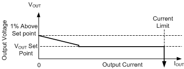
The LM61460 reduces frequency whenever output voltage is high. This function is enabled whenever Comp, an internal signal, is low and there is an offset between the regulation set point of FB and the voltage applied to FB. The net effect is that there is larger output impedance while lightly loaded in auto mode than in normal operation. Output voltage must be approximately 1% high when the part is completely unloaded.
GUID-FA99BD8B-2624-444B-8668-B7BF52CB3C6A-low.gif
In auto mode, once output current drops below approximately 1/10th the rated current of the part, output resistance increases so that output voltage is 1% high while the buck is completely unloaded.
Figure 8-18 Steady State Output Voltage Versus Output Current in Auto Mode

In PFM operation, a small DC positive offset is required on the output voltage to activate the PFM detector. The lower the frequency in PFM, the more DC offset is needed on VOUT. If the DC offset on VOUT is not acceptable, a dummy load at VOUT or FPWM Mode can be used to reduce or eliminate this offset.