SNVSBA0D February 2020 – August 2021 LM61480-Q1 , LM61495-Q1 , LM62460-Q1
PRODUCTION DATA
- 1 Features
- 2 Applications
- 3 Description
- 4 Revision History
- 5 Device Comparison Table
- 6 Pin Configuration and Functions
- 7 Specifications
-
8 Detailed Description
- 8.1 Overview
- 8.2 Functional Block Diagram
- 8.3
Feature Description
- 8.3.1 Output Voltage Selection
- 8.3.2 Enable EN Pin and Use as VIN UVLO
- 8.3.3 SYNC/MODE Uses for Synchronization
- 8.3.4 Clock Locking
- 8.3.5 Adjustable Switching Frequency
- 8.3.6 RESET Output Operation
- 8.3.7 Internal LDO, VCC UVLO, and BIAS Input
- 8.3.8 Bootstrap Voltage and VCBOOT-UVLO (CBOOT Pin)
- 8.3.9 Adjustable SW Node Slew Rate
- 8.3.10 Spread Spectrum
- 8.3.11 Soft Start and Recovery From Dropout
- 8.3.12 Overcurrent and Short Circuit Protection
- 8.3.13 Hiccup
- 8.3.14 Thermal Shutdown
- 8.4 Device Functional Modes
-
9 Application and Implementation
- 9.1 Application Information
- 9.2
Typical Application
- 9.2.1 Design Requirements
- 9.2.2
Detailed Design Procedure
- 9.2.2.1 Choosing the Switching Frequency
- 9.2.2.2 Setting the Output Voltage
- 9.2.2.3 Inductor Selection
- 9.2.2.4 Output Capacitor Selection
- 9.2.2.5 Input Capacitor Selection
- 9.2.2.6 BOOT Capacitor
- 9.2.2.7 BOOT Resistor
- 9.2.2.8 VCC
- 9.2.2.9 CFF and RFF Selection
- 9.2.2.10 RSPSP Selection
- 9.2.2.11 RT Selection
- 9.2.2.12 RMODE Selection
- 9.2.2.13 External UVLO
- 9.2.2.14 Maximum Ambient Temperature
- 9.2.3 Application Curves
- 10Power Supply Recommendations
- 11Layout
- 12Device and Documentation Support
- 13Mechanical, Packaging, and Orderable Information
Package Options
Mechanical Data (Package|Pins)
- RPH|16
Thermal pad, mechanical data (Package|Pins)
- RPH|16
Orderable Information
3 Description
The LM6x4xx-Q1 buck regulator family are automotive-focused regulators providing either fixed or an adjustable output voltage which can be set from 1 V to 95% of expected input voltage. These regulators operate under a wide input voltage range of 3 to 36V and has transient tolerance up to 42 V.
The family is designed for low EMI. The device incorporates pin selectable spread spectrum, and an adjustable SW node rise time. Dual Random Spread Spectrum (DRSS) frequency hopping is set to ±4% (typical), drastically reducing peak emissions through a combination of triangular and pseudorandom modulation, and includes advanced techniques to reduce output voltage ripple caused by spread spectrum modulation.
An open-drain RESET output, with filtering and delayed release, gives a true indication of system status. In auto mode the device automatically transitions between Fixed frequency Pulse Width Modulation (FPWM) and Pulse Frequency Modulation (PFM) modes of operation, allowing an unloaded current consumption of only 5 µA (typical). Electrical characteristics are specified over a junction temperature range of –40°C to +150°C.
| PART NUMBER | PACKAGE(1) | BODY SIZE (NOM) |
|---|---|---|
| LM61495-Q1 | VQFN (16) | 4.50 mm × 3.50 mm |
| LM61480-Q1 | ||
| LM62460-Q1 |
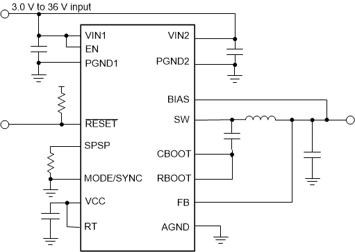
 Simplified Schematic