SNVSCR9A October 2024 – December 2024 LM61480T-Q1 , LM61495T-Q1
PRODUCTION DATA
- 1
- 1 Features
- 2 Applications
- 3 Description
- 4 Device Comparison Table
- 5 Pin Configuration and Functions
- 6 Specifications
-
7 Detailed Description
- 7.1 Overview
- 7.2 Functional Block Diagram
- 7.3
Feature Description
- 7.3.1 Output Voltage Selection
- 7.3.2 Enable EN Pin and Use as VIN UVLO
- 7.3.3 SYNC/MODE Uses for Synchronization
- 7.3.4 Clock Locking
- 7.3.5 Adjustable Switching Frequency
- 7.3.6 RESET Output Operation
- 7.3.7 Internal LDO, VCC UVLO, and BIAS Input
- 7.3.8 Bootstrap Voltage and VCBOOT-UVLO (CBOOT Pin)
- 7.3.9 Adjustable SW Node Slew Rate
- 7.3.10 Spread Spectrum
- 7.3.11 Soft Start and Recovery From Dropout
- 7.3.12 Overcurrent and Short-Circuit Protection
- 7.3.13 Hiccup
- 7.3.14 Thermal Shutdown
- 7.4 Device Functional Modes
-
8 Application and Implementation
- 8.1 Application Information
- 8.2
Typical Application
- 8.2.1 Design Requirements
- 8.2.2
Detailed Design Procedure
- 8.2.2.1 Choosing the Switching Frequency
- 8.2.2.2 Setting the Output Voltage
- 8.2.2.3 Inductor Selection
- 8.2.2.4 Output Capacitor Selection
- 8.2.2.5 Input Capacitor Selection
- 8.2.2.6 BOOT Capacitor
- 8.2.2.7 BOOT Resistor
- 8.2.2.8 VCC
- 8.2.2.9 CFF and RFF Selection
- 8.2.2.10 RSPSP Selection
- 8.2.2.11 RT Selection
- 8.2.2.12 RMODE Selection
- 8.2.2.13 External UVLO
- 8.2.2.14 Maximum Ambient Temperature
- 8.2.3 Application Curves
- 8.3 Power Supply Recommendations
- 8.4 Layout
- 9 Device and Documentation Support
- 10Revision History
- 11Mechanical, Packaging, and Orderable Information
Package Options
Mechanical Data (Package|Pins)
- VAM|16
Thermal pad, mechanical data (Package|Pins)
Orderable Information
7.3.11 Soft Start and Recovery From Dropout
When designing with the LM614xxT-Q1, slowed rise in output voltage due to recovery from dropout and soft start must be considered separate phenomena. Soft start is triggered by any of the following conditions:
- EN is used to turn on the device.
- Recovery from a hiccup waiting period; see Section 7.3.13.
- Recovery from shutdown due to overtemperature protection.
- Power is applied to the VIN of the IC or the VCC UVLO is released.
After soft start is triggered, the IC takes the following actions:
- The reference used by the IC to regulate output voltage is slowly ramped from zero. The net result is that output voltage, if previously 0V, takes tSS to reach 90% of the desired value.
- Operating mode is set to auto, activating diode emulation. This action allows start-up without pulling output low if there is a voltage already present on the output.
- Hiccup is disabled for the duration of soft start; see Section 7.3.13.
All of these actions together provide start-up with limited inrush currents. These actions also allow the use of output capacitors and loading conditions that cause current to border on current limit during start-up without triggering hiccup. In addition, if output voltage is already present, output is not pulled down. See Figure 7-13.

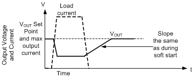
Any time output voltage is more than a few percent low for any reason, output voltage ramps up slowly. This condition, called recovery from dropout, differs from soft start in three important ways:
- Hiccup is allowed only if output voltage is less than 0.4 times the set point. Note that during dropout regulation, hiccup is inhibited. See Section 7.3.13.
- FPWM mode is allowed during recovery from dropout. If output voltage were to suddenly be pulled up by an external supply, the LM614xxT-Q1 can pull down on the output. Note that all the protections that are present during normal operation are in place, protecting the device if output is shorted to a high voltage or ground.
- The reference voltage is set to approximately 1% above that needed to achieve the current output voltage. The reference voltage is not started from zero.
Despite the name, recovery from dropout is active whenever output voltage is more than a few percent lower than the setpoint for long enough that:
- Duty factor is controlled by minimum on-time or
- When the part is operating in current limit.
- Dropout: when there is insufficient input voltage for the desired output voltage to be generated. See Section 7.4.3.5.
- Overcurrent that is not severe enough to trigger hiccup or if the duration is too short to trigger hiccup. See Section 7.3.13.
