SNVSCR9 October 2024 LM61495T-Q1
ADVANCE INFORMATION
- 1
- 1 Features
- 2 Applications
- 3 Description
- 4 Device Comparison Table
- 5 Pin Configuration and Functions
- 6 Specifications
-
7 Detailed Description
- 7.1 Overview
- 7.2 Functional Block Diagram
- 7.3
Feature Description
- 7.3.1 Output Voltage Selection
- 7.3.2 Enable EN Pin and Use as VIN UVLO
- 7.3.3 SYNC/MODE Uses for Synchronization
- 7.3.4 Clock Locking
- 7.3.5 Adjustable Switching Frequency
- 7.3.6 RESET Output Operation
- 7.3.7 Internal LDO, VCC UVLO, and BIAS Input
- 7.3.8 Bootstrap Voltage and VCBOOT-UVLO (CBOOT Pin)
- 7.3.9 Adjustable SW Node Slew Rate
- 7.3.10 Spread Spectrum
- 7.3.11 Soft Start and Recovery From Dropout
- 7.3.12 Overcurrent and Short-Circuit Protection
- 7.3.13 Hiccup
- 7.3.14 Thermal Shutdown
- 7.4 Device Functional Modes
-
8 Application and Implementation
- 8.1 Application Information
- 8.2
Typical Application
- 8.2.1 Design Requirements
- 8.2.2
Detailed Design Procedure
- 8.2.2.1 Choosing the Switching Frequency
- 8.2.2.2 Setting the Output Voltage
- 8.2.2.3 Inductor Selection
- 8.2.2.4 Output Capacitor Selection
- 8.2.2.5 Input Capacitor Selection
- 8.2.2.6 BOOT Capacitor
- 8.2.2.7 BOOT Resistor
- 8.2.2.8 VCC
- 8.2.2.9 CFF and RFF Selection
- 8.2.2.10 RSPSP Selection
- 8.2.2.11 RT Selection
- 8.2.2.12 RMODE Selection
- 8.2.2.13 External UVLO
- 8.2.2.14 Maximum Ambient Temperature
- 8.2.3 Application Curves
- 8.3 Power Supply Recommendations
- 8.4 Layout
- 9 Device and Documentation Support
- 10Revision History
- 11Mechanical, Packaging, and Orderable Information
Package Options
Mechanical Data (Package|Pins)
- VAM|16
Thermal pad, mechanical data (Package|Pins)
Orderable Information
7.3.13 Hiccup
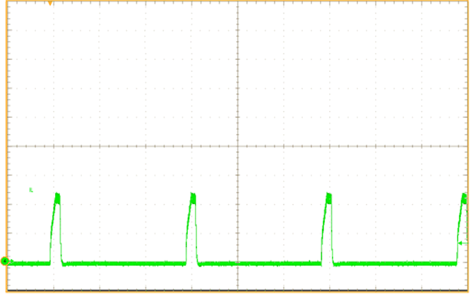
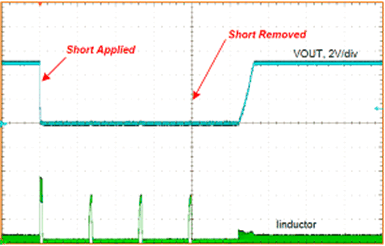
The LM614xxT-Q1 employs hiccup overcurrent protection when all of the following conditions are met for 128 consecutive switching cycles:
- A time greater than tSS2 has passed since soft start has started; see Section 7.3.11.
- Output voltage is below approximately 0.4 times output setpoint.
- The part is not operating in dropout defined as having minimum off-time controlled by duty factor.
In hiccup mode, the device shuts down and attempts to soft start after tW. Hiccup mode helps reduce the device power dissipation under severe overcurrent conditions and short circuits.
 Figure 7-18 Inductor Current Bursts During Hiccup
 Figure 7-19 Short-Circuit Transient and Recovery