SNOS745D May   1998  – November 2023 LM6171

PRODUCTION DATA  

  1.   1
  2. Features
  3. Applications
  4. Description
  5. Pin Configuration and Functions
  6. Specifications
    1. 5.1 Absolute Maximum Ratings
    2. 5.2 ESD Ratings
    3. 5.3 Recommended Operating Conditions
    4. 5.4 Thermal Information
    5. 5.5 Electrical Characteristics: ±15 V
    6. 5.6 Electrical Characteristics: ±5 V
    7. 5.7 Typical Characteristics: LM6171A Only
    8. 5.8 Typical Characteristics
  7. Detailed Description
    1. 6.1 Overview
    2. 6.2 Functional Block Diagram
    3. 6.3 Feature Description
      1. 6.3.1 Circuit Operation
      2. 6.3.2 Slew Rate
    4. 6.4 Device Functional Modes
  8. Application and Implementation
    1. 7.1 Application Information
      1. 7.1.1 Compensation for Input Capacitance
      2. 7.1.2 Power Supply Bypassing
      3. 7.1.3 Termination
      4. 7.1.4 Driving Capacitive Loads
      5. 7.1.5 Using Probes
      6. 7.1.6 Components Selection and Feedback Resistor
    2. 7.2 Typical Applications
      1. 7.2.1 Fast Instrumentation Amplifier
      2. 7.2.2 Multivibrator
      3. 7.2.3 Pulse Width Modulator
    3. 7.3 Power Supply Recommendations
      1. 7.3.1 Power Dissipation
    4. 7.4 Layout
      1. 7.4.1 Layout Guidelines
        1. 7.4.1.1 Printed Circuit Boards and High-Speed Op Amps
  9. Device and Documentation Support
    1. 8.1 Receiving Notification of Documentation Updates
    2. 8.2 Support Resources
    3. 8.3 Trademarks
    4. 8.4 Electrostatic Discharge Caution
    5. 8.5 Glossary
  10. Revision History
  11. 10Mechanical, Packaging, and Orderable Information

Package Options

Refer to the PDF data sheet for device specific package drawings

Mechanical Data (Package|Pins)
  • D|8
  • P|8
Thermal pad, mechanical data (Package|Pins)
Orderable Information

Pin Configuration and Functions

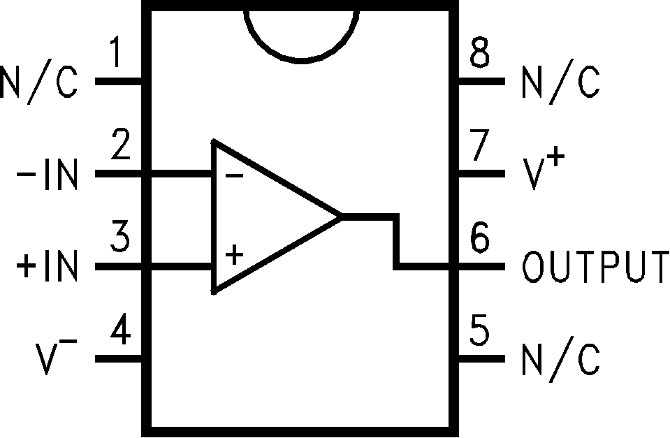
GUID-B58579F8-CE52-468E-8833-3E72DDA213C3-low.png Figure 4-1 D Package, 8-Pin SOIC
P Package, 8-Pin PDIP
(Top View)
Table 4-1 Pin Functions
PIN TYPE(1) DESCRIPTION
NAME NO.
–IN 2 I Negative input pin
+IN 3 I Positive input pin
N/C 1, 5, 8 This pin is not internally connected; leave floating or connect to any other pin on the device.
OUTPUT 6 O Output pin.
V 4 I/O Negative supply voltage pin.
V+ 7 I/O Positive supply voltage pin.
Signal types: I = input, O = output, I/O = input or output.