SNOS792E May 1999 – December 2024 LM6172
PRODUCTION DATA
- 1
- 1 Features
- 2 Applications
- 3 Description
- 4 Pin Configuration and Functions
- 5 Specifications
- 6 Detailed Description
- 7 Application and Implementation
- 8 Device and Documentation Support
- 9 Revision History
- 10Mechanical, Packaging, and Orderable Information
Package Options
Refer to the PDF data sheet for device specific package drawings
Mechanical Data (Package|Pins)
- D|8
- P|8
Thermal pad, mechanical data (Package|Pins)
Orderable Information
3 Description
The LM6172 is a dual, high-speed voltage-feedback amplifier. The device is unity-gain stable and provides excellent dc and ac performance. With a 100MHz unity-gain bandwidth, 3000V/μs slew rate, and 50mA of output current per channel, the LM6172 offers high performance in dual amplifiers, yet only consumes 2.3mA of supply current per channel.
The LM6172 operates on ±15V power supplies for systems requiring large voltage swings, such as ADSL, scanners and ultrasound equipment. The device is also specified for ±5‑V power supplies for low-voltage applications, such as portable video systems.
The LM6172 is built with TI's advanced complementary bipolar process. See the LM6171 data sheet for a single amplifier with these same features.
| PART NUMBER | PACKAGE(1) | PACKAGE SIZE(2) |
|---|---|---|
| LM6172 | D (SOIC, 8) | 4.9mm × 6mm |
| P (PDIP, 8) | 9.81mm × 9.43mm |
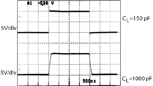
 LM6172 Driving a Capacitive Load
 LM6172
Driving Capacitive Load