SNOS792E May   1999  – December 2024 LM6172

PRODUCTION DATA  

  1.   1
  2. Features
  3. Applications
  4. Description
  5. Pin Configuration and Functions
  6. Specifications
    1. 5.1 Absolute Maximum Ratings
    2. 5.2 ESD Ratings
    3. 5.3 Recommended Operating Conditions
    4. 5.4 Thermal Information
    5. 5.5 Electrical Characteristics ±15V
    6. 5.6 Electrical Characteristics ±5V
    7. 5.7 Typical Characteristics: D (SOIC, 8) Package
    8. 5.8 Typical Characteristics: P (PDIP, 8) Package
  7. Detailed Description
    1. 6.1 Overview
    2. 6.2 Functional Block Diagram
    3. 6.3 Feature Description
      1. 6.3.1 Slew Rate
  8. Application and Implementation
    1. 7.1 Application Information
      1. 7.1.1 Circuit Operation
      2. 7.1.2 Reduce Settling Time
      3. 7.1.3 Drive Capacitive Loads
      4. 7.1.4 Compensation for Input Capacitance
      5. 7.1.5 Termination
    2. 7.2 Typical Application
      1. 7.2.1 Application Circuits
    3. 7.3 Power Supply Recommendations
      1. 7.3.1 Power Supply Bypassing
      2. 7.3.2 Power Dissipation
    4. 7.4 Layout
      1. 7.4.1 Layout Guidelines
        1. 7.4.1.1 Printed Circuit Boards and High-Speed Op Amps
        2. 7.4.1.2 Using Probes
        3. 7.4.1.3 Components Selection and Feedback Resistor
  9. Device and Documentation Support
    1. 8.1 Receiving Notification of Documentation Updates
    2. 8.2 Support Resources
    3. 8.3 Trademarks
    4. 8.4 Electrostatic Discharge Caution
    5. 8.5 Glossary
  10. Revision History
  11. 10Mechanical, Packaging, and Orderable Information

Package Options

Refer to the PDF data sheet for device specific package drawings

Mechanical Data (Package|Pins)
  • D|8
  • P|8
Thermal pad, mechanical data (Package|Pins)
Orderable Information

Compensation for Input Capacitance

The combination of an amplifier input capacitance with gain-setting resistors adds a pole that can cause peaking or oscillation. To solve this problem, a feedback capacitor with the following value can be used to cancel that pole:

Equation 1. CF > (RG × CIN) / RF

For the LM6172, a feedback capacitor of 2pF is recommended. Figure 7-4 illustrates the compensation circuit.
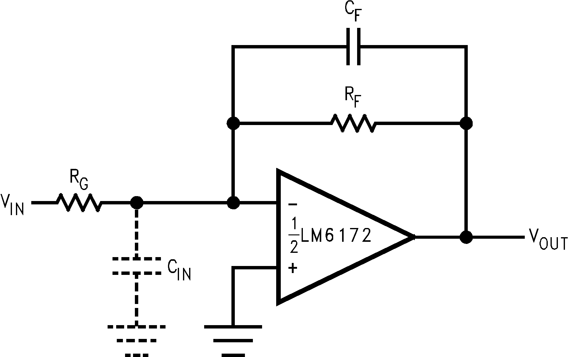
LM6172 Compensating for Input CapacitanceFigure 7-4 Compensating for Input Capacitance