SNVSBO7A July   2020  – July 2021 LM63610-Q1

PRODUCTION DATA  

  1. Features
  2. Applications
  3. Description
  4. Revision History
  5. Device Comparison Table
  6. Pin Configuration and Functions
  7. Specifications
    1. 7.1 Absolute Maximum Ratings
    2. 7.2 ESD Ratings
    3. 7.3 Recommended Operating Conditions
    4. 7.4 Thermal Information
    5. 7.5 Electrical Characteristics
    6. 7.6 Timing Characteristics
    7. 7.7 Switching Characteristics
    8. 7.8 System Characteristics
    9. 7.9 Typical Characteristics
  8. Detailed Description
    1. 8.1 Overview
    2. 8.2 Functional Block Diagram
    3. 8.3 Feature Description
      1. 8.3.1 Sync/Mode Selection
      2. 8.3.2 Output Voltage Selection
      3. 8.3.3 Switching Frequency Selection
        1. 8.3.3.1 Spread Spectrum Option
      4. 8.3.4 Enable and Start-up
      5. 8.3.5 RESET Flag Output
      6. 8.3.6 Undervoltage Lockout and Thermal Shutdown and Output Discharge
    4. 8.4 Device Functional Modes
      1. 8.4.1 Overview
      2. 8.4.2 Light Load Operation
        1. 8.4.2.1 Sync/FPWM Operation
      3. 8.4.3 Dropout Operation
      4. 8.4.4 Minimum On-time Operation
      5. 8.4.5 Current Limit and Short-Circuit Operation
  9. Application and Implementation
    1. 9.1 Application Information
    2. 9.2 Typical Application
      1. 9.2.1 Design Requirements
      2. 9.2.2 Detailed Design Procedure
        1. 9.2.2.1 Choosing the Switching Frequency
        2. 9.2.2.2 Setting the Output Voltage
          1. 9.2.2.2.1 CFF Selection
        3. 9.2.2.3 Inductor Selection
        4. 9.2.2.4 Output Capacitor Selection
        5. 9.2.2.5 Input Capacitor Selection
        6. 9.2.2.6 CBOOT
        7. 9.2.2.7 VCC
        8. 9.2.2.8 External UVLO
        9. 9.2.2.9 Maximum Ambient Temperature
      3. 9.2.3 Application Curves
      4. 9.2.4 EMI Performance Curves
    3. 9.3 What to Do and What Not to Do
  10. 10Power Supply Recommendations
  11. 11Layout
    1. 11.1 Layout Guidelines
      1. 11.1.1 Ground and Thermal Considerations
    2. 11.2 Layout Example
  12. 12Device and Documentation Support
    1. 12.1 Documentation Support
      1. 12.1.1 Related Documentation
    2. 12.2 Receiving Notification of Documentation Updates
    3. 12.3 Support Resources
    4. 12.4 Trademarks
    5. 12.5 Electrostatic Discharge Caution
    6. 12.6 Glossary
  13. 13Mechanical, Packaging, and Orderable Information

Package Options

Mechanical Data (Package|Pins)
Thermal pad, mechanical data (Package|Pins)
Orderable Information

Description

The LM63610-Q1 regulators are a family of easy-to-use, synchronous, step-down DC/DC converters designed for rugged automotive applications. The LM63610-Q1 can drive up to 1 A of load current from an input of up to 36 V. The converter has high light load efficiency and output accuracy in a small solution size. Features such as a RESET flag and precision enable provide both flexible and easy-to-use solutions for a wide range of applications. Automatic frequency foldback at light load improves efficiency while maintaining tight load regulation. Integration eliminates many external components and provides a pinout designed for simple PCB layout. Protection features include thermal shutdown, input undervoltage lockout, cycle-by-cycle current limit, and hiccup short-circuit protection. The LM63610-Q1 is available in both the HTSSOP 16-pin power package, with PowerPAD™, and the WSON 12-pin power package. Please contact Texas Instruments for availability of the WSON package.

Device Information
PART NUMBERPACKAGE(1)BODY SIZE (NOM)
LM63610-Q1HTSSOP (16)5.00 mm × 4.00 mm
LM63610-Q1WSON (12)3.00 mm × 3.00 mm
For all available packages, see the orderable addendum at the end of the data sheet.
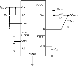
GUID-E3AC70B6-BE82-48FB-9E2C-5AFE7371A5B5-low.gifSimplified Schematic
GUID-D7EAB54E-7BD0-4417-B976-CFB61193BBFB-low.gifTypical Efficiency At 5-V Vout, 2.1 MHz