SNVSBO7A July 2020 – July 2021 LM63610-Q1
PRODUCTION DATA
- 1 Features
- 2 Applications
- 3 Description
- 4 Revision History
- 5 Device Comparison Table
- 6 Pin Configuration and Functions
- 7 Specifications
- 8 Detailed Description
- 9 Application and Implementation
- 10Power Supply Recommendations
- 11Layout
- 12Device and Documentation Support
- 13Mechanical, Packaging, and Orderable Information
Package Options
Mechanical Data (Package|Pins)
Thermal pad, mechanical data (Package|Pins)
Orderable Information
8.3.4 Enable and Start-up
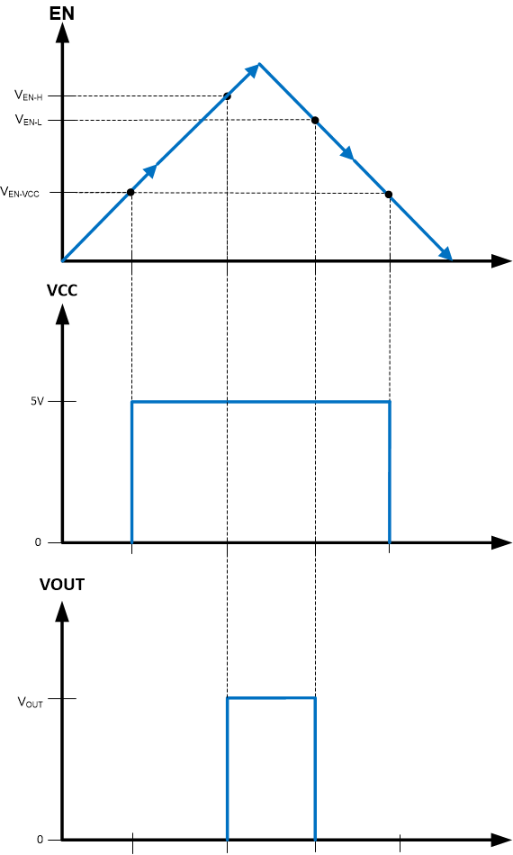
Start-up and shutdown are controlled by the EN input. This input features precision thresholds, allowing the use of an external voltage divider to provide an adjustable input UVLO (see External UVLO). Applying a voltage greater than VEN-VCC causes the device to enter standby mode, powering the internal VCC, but not producing an output voltage. Increasing the EN voltage to VEN-H fully enables the device, allowing it to enter start-up mode and begin the soft-start period. When the EN input is brought below VEN-L, the regulator stops running and enters standby mode. Further decrease in the EN voltage to below VEN-VCC completely shuts down the device. Figure 8-2 shows this behavior. The EN input can be connected directly to VIN if this feature is not needed. This input must not be allowed to float. The values for the various EN thresholds can be found in Specifications .
The LM63610-Q1 uses a reference-based soft start that prevents output voltage overshoots and large inrush currents as the regulator is starting up. Once EN goes high, there is a delay of about 1 ms before the soft-start period begins. The output voltage begins to rise and reaches the final value in about 1.5 ms (tss). After a delay of about 3 ms (trise-delay), the RESET flag goes high. During start-up, the device is not allowed to enter FPWM mode until the tss-done time has elapsed. This time is measured from the rising edge of EN.
 Figure 8-2 Precision Enable Behavior