SNVSBK9G November   2019  – November 2024 LM63635-Q1

PRODUCTION DATA  

  1.   1
  2. Features
  3. Applications
  4. Description
  5. Device Comparison Table
  6. Pin Configuration and Functions
  7. Specifications
    1. 6.1 Absolute Maximum Ratings
    2. 6.2 ESD Ratings
    3. 6.3 Recommended Operating Conditions
    4. 6.4 Thermal Information
    5. 6.5 Electrical Characteristics
    6. 6.6 Timing Characteristics
    7. 6.7 Switching Characteristics
    8. 6.8 System Characteristics
    9. 6.9 Typical Characteristics
  8. Detailed Description
    1. 7.1 Overview
    2. 7.2 Functional Block Diagram
    3. 7.3 Feature Description
      1. 7.3.1 Sync/Mode Selection
      2. 7.3.2 Output Voltage Selection
      3. 7.3.3 Switching Frequency Selection
        1. 7.3.3.1 Spread Spectrum Option
      4. 7.3.4 Enable and Start-Up
      5. 7.3.5 RESET Flag Output
      6. 7.3.6 Undervoltage Lockout and Thermal Shutdown and Output Discharge
    4. 7.4 Device Functional Modes
      1. 7.4.1 Overview
      2. 7.4.2 Light Load Operation
        1. 7.4.2.1 Sync/FPWM Operation
      3. 7.4.3 Dropout Operation
      4. 7.4.4 Minimum On-time Operation
      5. 7.4.5 Current Limit and Short-Circuit Operation
  9. Application and Implementation
    1. 8.1 Application Information
    2. 8.2 Typical Application
      1. 8.2.1 Design Requirements
      2. 8.2.2 Detailed Design Procedure
        1. 8.2.2.1 Choosing the Switching Frequency
        2. 8.2.2.2 Setting the Output Voltage
          1. 8.2.2.2.1 CFF Selection
        3. 8.2.2.3 Inductor Selection
        4. 8.2.2.4 Output Capacitor Selection
        5. 8.2.2.5 Input Capacitor Selection
        6. 8.2.2.6 CBOOT
        7. 8.2.2.7 VCC
        8. 8.2.2.8 External UVLO
        9. 8.2.2.9 Maximum Ambient Temperature
      3. 8.2.3 Full Feature Design Example
      4. 8.2.4 Application Curves
      5. 8.2.5 EMI Performance Curves
    3. 8.3 Best Design Practices
    4. 8.4 Power Supply Recommendations
    5. 8.5 Layout
      1. 8.5.1 Layout Guidelines
        1. 8.5.1.1 Ground and Thermal Considerations
      2. 8.5.2 Layout Example
  10. Device and Documentation Support
    1. 9.1 Device Support
      1. 9.1.1 Device Nomenclature
    2. 9.2 Documentation Support
      1. 9.2.1 Related Documentation
    3. 9.3 Receiving Notification of Documentation Updates
    4. 9.4 Support Resources
    5. 9.5 Trademarks
    6. 9.6 Electrostatic Discharge Caution
    7. 9.7 Glossary
  11. 10Revision History
  12. 11Mechanical, Packaging, and Orderable Information

Package Options

Mechanical Data (Package|Pins)
Thermal pad, mechanical data (Package|Pins)
Orderable Information

Switching Frequency Selection

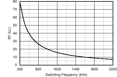
The switching frequency is set by the condition of the RT input. The condition of this input is tested when the device is first enabled. After the converter is running, the switching frequency selection is fixed and cannot be changed until the next power-on cycle. Table 7-3 shows the selection programming. In the adjustable frequency mode, the switching frequency can be set between 250 kHz and 2200 kHz by proper selection of the value of RT. The curve in Figure 7-1 indicates the required resistor value for RT to set a desired switching frequency. TI does not recommend that this input be allowed to float; the switching action ceases with no generated output voltage under this condition.

Equation 1. R T = 15770 f S W

where

  • RT = value of RT timing resistor in kΩ
  • ƒSW = switching frequency in kHz
Table 7-3 Switching Frequency Settings
RT INPUTSWITCHING FREQUENCY
VCC400 kHz
AGND2100 kHz
RT to AGNDAdjustable according to RT value
Float (not recommended)No switching
LM63635-Q1 Switching Frequency versus RTFigure 7-1 Switching Frequency versus RT