SNVSBK9G November   2019  – November 2024 LM63635-Q1

PRODUCTION DATA  

  1.   1
  2. Features
  3. Applications
  4. Description
  5. Device Comparison Table
  6. Pin Configuration and Functions
  7. Specifications
    1. 6.1 Absolute Maximum Ratings
    2. 6.2 ESD Ratings
    3. 6.3 Recommended Operating Conditions
    4. 6.4 Thermal Information
    5. 6.5 Electrical Characteristics
    6. 6.6 Timing Characteristics
    7. 6.7 Switching Characteristics
    8. 6.8 System Characteristics
    9. 6.9 Typical Characteristics
  8. Detailed Description
    1. 7.1 Overview
    2. 7.2 Functional Block Diagram
    3. 7.3 Feature Description
      1. 7.3.1 Sync/Mode Selection
      2. 7.3.2 Output Voltage Selection
      3. 7.3.3 Switching Frequency Selection
        1. 7.3.3.1 Spread Spectrum Option
      4. 7.3.4 Enable and Start-Up
      5. 7.3.5 RESET Flag Output
      6. 7.3.6 Undervoltage Lockout and Thermal Shutdown and Output Discharge
    4. 7.4 Device Functional Modes
      1. 7.4.1 Overview
      2. 7.4.2 Light Load Operation
        1. 7.4.2.1 Sync/FPWM Operation
      3. 7.4.3 Dropout Operation
      4. 7.4.4 Minimum On-time Operation
      5. 7.4.5 Current Limit and Short-Circuit Operation
  9. Application and Implementation
    1. 8.1 Application Information
    2. 8.2 Typical Application
      1. 8.2.1 Design Requirements
      2. 8.2.2 Detailed Design Procedure
        1. 8.2.2.1 Choosing the Switching Frequency
        2. 8.2.2.2 Setting the Output Voltage
          1. 8.2.2.2.1 CFF Selection
        3. 8.2.2.3 Inductor Selection
        4. 8.2.2.4 Output Capacitor Selection
        5. 8.2.2.5 Input Capacitor Selection
        6. 8.2.2.6 CBOOT
        7. 8.2.2.7 VCC
        8. 8.2.2.8 External UVLO
        9. 8.2.2.9 Maximum Ambient Temperature
      3. 8.2.3 Full Feature Design Example
      4. 8.2.4 Application Curves
      5. 8.2.5 EMI Performance Curves
    3. 8.3 Best Design Practices
    4. 8.4 Power Supply Recommendations
    5. 8.5 Layout
      1. 8.5.1 Layout Guidelines
        1. 8.5.1.1 Ground and Thermal Considerations
      2. 8.5.2 Layout Example
  10. Device and Documentation Support
    1. 9.1 Device Support
      1. 9.1.1 Device Nomenclature
    2. 9.2 Documentation Support
      1. 9.2.1 Related Documentation
    3. 9.3 Receiving Notification of Documentation Updates
    4. 9.4 Support Resources
    5. 9.5 Trademarks
    6. 9.6 Electrostatic Discharge Caution
    7. 9.7 Glossary
  11. 10Revision History
  12. 11Mechanical, Packaging, and Orderable Information

Package Options

Mechanical Data (Package|Pins)
Thermal pad, mechanical data (Package|Pins)
Orderable Information

Sync/FPWM Operation

The forced PWM mode (FPWM) can be used to turn off AUTO mode and force the device to switch at the frequency programmed by the RT pin, even for small loads. This has the disadvantage of lower efficiency at light loads.

When a valid clock signal is present on the SYNC/MODE input, the switching frequency is locked to the external clock. The device mode is also FPWM. The mode can be changed dynamically by the system. See Figure 7-10 for typical examples of SYNC/MODE function changes.
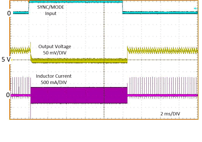
LM63635-Q1 Typical
                    Transition from FPWM to AUTO Mode VIN = 12 V, VOUT = 5 V,
                        IOUT = 1 mA Figure 7-10 Typical Transition from FPWM to AUTO Mode VIN = 12 V, VOUT = 5 V, IOUT = 1 mA