SNVSBK9G November   2019  – November 2024 LM63635-Q1

PRODUCTION DATA  

  1.   1
  2. Features
  3. Applications
  4. Description
  5. Device Comparison Table
  6. Pin Configuration and Functions
  7. Specifications
    1. 6.1 Absolute Maximum Ratings
    2. 6.2 ESD Ratings
    3. 6.3 Recommended Operating Conditions
    4. 6.4 Thermal Information
    5. 6.5 Electrical Characteristics
    6. 6.6 Timing Characteristics
    7. 6.7 Switching Characteristics
    8. 6.8 System Characteristics
    9. 6.9 Typical Characteristics
  8. Detailed Description
    1. 7.1 Overview
    2. 7.2 Functional Block Diagram
    3. 7.3 Feature Description
      1. 7.3.1 Sync/Mode Selection
      2. 7.3.2 Output Voltage Selection
      3. 7.3.3 Switching Frequency Selection
        1. 7.3.3.1 Spread Spectrum Option
      4. 7.3.4 Enable and Start-Up
      5. 7.3.5 RESET Flag Output
      6. 7.3.6 Undervoltage Lockout and Thermal Shutdown and Output Discharge
    4. 7.4 Device Functional Modes
      1. 7.4.1 Overview
      2. 7.4.2 Light Load Operation
        1. 7.4.2.1 Sync/FPWM Operation
      3. 7.4.3 Dropout Operation
      4. 7.4.4 Minimum On-time Operation
      5. 7.4.5 Current Limit and Short-Circuit Operation
  9. Application and Implementation
    1. 8.1 Application Information
    2. 8.2 Typical Application
      1. 8.2.1 Design Requirements
      2. 8.2.2 Detailed Design Procedure
        1. 8.2.2.1 Choosing the Switching Frequency
        2. 8.2.2.2 Setting the Output Voltage
          1. 8.2.2.2.1 CFF Selection
        3. 8.2.2.3 Inductor Selection
        4. 8.2.2.4 Output Capacitor Selection
        5. 8.2.2.5 Input Capacitor Selection
        6. 8.2.2.6 CBOOT
        7. 8.2.2.7 VCC
        8. 8.2.2.8 External UVLO
        9. 8.2.2.9 Maximum Ambient Temperature
      3. 8.2.3 Full Feature Design Example
      4. 8.2.4 Application Curves
      5. 8.2.5 EMI Performance Curves
    3. 8.3 Best Design Practices
    4. 8.4 Power Supply Recommendations
    5. 8.5 Layout
      1. 8.5.1 Layout Guidelines
        1. 8.5.1.1 Ground and Thermal Considerations
      2. 8.5.2 Layout Example
  10. Device and Documentation Support
    1. 9.1 Device Support
      1. 9.1.1 Device Nomenclature
    2. 9.2 Documentation Support
      1. 9.2.1 Related Documentation
    3. 9.3 Receiving Notification of Documentation Updates
    4. 9.4 Support Resources
    5. 9.5 Trademarks
    6. 9.6 Electrostatic Discharge Caution
    7. 9.7 Glossary
  11. 10Revision History
  12. 11Mechanical, Packaging, and Orderable Information

Package Options

Mechanical Data (Package|Pins)
Thermal pad, mechanical data (Package|Pins)
Orderable Information

Typical Characteristics

Unless otherwise specified the following conditions apply: TA = 25°C, VIN = 13.5 V
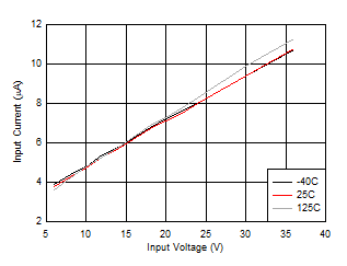
LM63635-Q1 Input Supply Current in Shutdown Mode
EN = 0 V
Figure 6-1 Input Supply Current in Shutdown Mode
LM63635-Q1 UVLO
                        Thresholds
IOUT = 1 mA See Figure 8-26
Figure 6-2 UVLO Thresholds