SNVSCO0 January 2024 LM63635C-Q1
PRODUCTION DATA
- 1
- 1 Features
- 2 Applications
- 3 Description
- 4 Device Comparison Table
- 5 Pin Configuration and Functions
- 6 Specifications
- 7 Detailed Description
- 8 Application and Implementation
- 9 Device and Documentation Support
- 10Revision History
- 11Mechanical, Packaging, and Orderable Information
Package Options
Mechanical Data (Package|Pins)
- DRR|12
Thermal pad, mechanical data (Package|Pins)
- DRR|12
Orderable Information
7.4.3 Dropout Operation
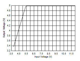
The dropout performance of any buck regulator is affected by the RDSON of the power MOSFETs, the DC resistance of the inductor, and the maximum duty cycle that the controller can achieve. As the input voltage level approaches the output voltage, the off-time of the high-side MOSFET starts to approach the minimum value (see Section 6). Beyond this point, the switching can become erratic and the output voltage can fall out of regulation. To avoid this problem, the LM63635C-Q1 automatically reduces the switching frequency to increase the effective duty cycle and maintain regulation. There are two definitions of dropout voltage used in this data sheet. For both definitions, the dropout voltage is the difference between the input and output voltage under a specific condition. For the first definition, the difference is taken when the switching frequency has dropped to 1850kHz (this applies to cases where the nominal switching frequency is > 1850kHz). For this condition, the output voltage is within regulation. For the second definition, the difference is taken when the output voltage has fallen by 1% of the nominal regulation value. In this condition, the switching frequency has reached the lower limit of about 130kHz. See Section 8.2.3 for details on these characteristics. Typical overall dropout characteristics can be found in Figure 7-8.
 Figure 7-8 Overall
Dropout Characteristic VOUT = 5V, IOUT = 3.25A