SNAS207B May 2004 – January 2024 LM64
PRODUCTION DATA
- 1
- 1 Features
- 2 Applications
- 3 Description
- 4 Pin Configuration and Functions
- 5 Specifications
-
6 Detailed Description
- 6.1 Overview
- 6.2 Functional Block Diagram
- 6.3
Feature Description
- 6.3.1 Conversion Sequence
- 6.3.2 The ALERT Output
- 6.3.3 SMBus Interface
- 6.3.4 Power-On Reset (POR) Default States
- 6.3.5 Temperature Data Format
- 6.3.6 Open-Drain Outputs, Inputs, and Pull-Up Resistors
- 6.3.7 Diode Fault Detection
- 6.3.8 Communicating with the LM64
- 6.3.9 Digital Filter
- 6.3.10 Fault Queue
- 6.3.11 One-Shot Register
- 6.3.12 Serial Interface Reset
-
7 Registers
- 7.1
LM64 Registers
- 7.1.1 LM64 Register Map in Hexadecimal Order
- 7.1.2 LM64 Register Map in Functional Order
- 7.1.3 LM64 Initial Register Sequence and Register Descriptions in Functional Order
- 7.1.4
LM64 Register Descriptions in Functional Order
- 7.1.4.1 Fan Control Registers
- 7.1.4.2 Configuration Register
- 7.1.4.3 Tachometer Count And Limit Registers
- 7.1.4.4 Local Temperature And Local High Setpoint Registers
- 7.1.4.5 Remote Diode Temperature, Offset And Setpoint Registers
- 7.1.4.6 ALERT Status And Mask Registers
- 7.1.4.7 Conversion Rate And One-Shot Registers
- 7.1.4.8 ID Registers
- 7.2 General Purpose Registers
- 7.1
LM64 Registers
- 8 Application and Implementation
- 9 Layout
- 10Device and Documentation Support
- 11Revision History
- 12Mechanical, Packaging, and Orderable Information
Package Options
Mechanical Data (Package|Pins)
- NHW|24
Thermal pad, mechanical data (Package|Pins)
Orderable Information
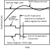
6.3.2.2 ALERT Output as an Interrupt
The LM64's ALERT output can be implemented as a simple interrupt signal when it is used to trigger an interrupt service routine. In such systems it is desirable for the interrupt flag to repeatedly trigger during or before the interrupt service routine has been completed. Under this method of operation, during the read of the ALERT Status Register the LM64 will set the ALERT Mask bit in the Configuration Register if any bit in the ALERT Status Register is set, with the exception of Busy and Open. This prevents further ALERT triggering until the master has reset the ALERT Mask bit, at the end of the interrupt service routine. The ALERT Status Register bits are cleared only upon a read command from the master (see Figure 6-2) and will be re-asserted at the end of the next conversion if the triggering condition(s) persist(s). In order for the ALERT to be used as a dedicated interrupt signal, the Comparator Mode bit in the Remote Diode Temperature Filter and Comparator Mode Register must be set low. This is the power-on default state. The following sequence describes the response of a system that uses the ALERT output pin as an interrupt flag:
- Master senses ALERT low.
- Master reads the LM64 ALERT Status Register to determine what caused the ALERT.
- LM64 clears ALERT Status Register, resets the ALERT HIGH and sets the ALERT Mask bit in the Configuration Register.
- Master attends to conditions that caused the ALERT to be triggered. The fan is started, setpoint limits are adjusted, etc.
- Master resets the ALERT Mask bit in the Configuration Register.
 Figure 6-3 ALERT Output as an Interrupt Temperature Response Diagram